 ALLPCB


Introduction
Panel fiducials play a pivotal role in surface mount technology assembly for panelized printed circuit boards. These reference marks allow pick-and-place machines to achieve precise alignment by correcting for translational, rotational, and nonlinear distortions across the entire panel. As component density increases in modern designs, engineers must navigate SMT design constraints to preserve PCB real estate for active components. Poor fiducial mark design can lead to misalignment errors, reducing yield and increasing rework costs. Effective fiducial mark design optimizes space while maintaining sub-micron placement accuracy essential for high-volume production. This article explores strategies for balancing these competing demands.
What Are Panel Fiducials and Why Do They Matter?
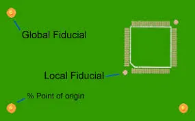
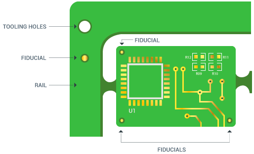
Panel fiducials are dedicated copper features placed on the outer frame of a multi-board panel to establish a common reference datum for the entire array during automated assembly. Unlike global fiducials on individual boards or local fiducials near fine-pitch components, panel fiducials ensure uniform alignment across all boards in the panel, compensating for panel-scale warpage or scaling errors. In high component density designs, these marks become critical as SMT machines rely on them to achieve placement accuracies below 25 microns. Without proper panel fiducials, assembly errors propagate, exacerbating issues like tombstoning or bridging in dense layouts. Their importance grows with panelization for cost efficiency in medium-to-high volumes. Designers must integrate them thoughtfully to avoid compromising PCB real estate.
The relevance stems from evolving SMT design constraints, where boards pack more functionality into smaller footprints. Fiducials enable machine vision systems to detect board orientation and position, preventing flipped or rotated placements. In panels, typically three fiducials form a non-collinear triangle for full six-degree-of-freedom correction. This setup directly impacts space optimization, as each fiducial requires a dedicated clearance zone free of other features. Neglecting panel fiducials risks production halts, underscoring their necessity in professional engineering workflows.
Technical Principles of Fiducial Mark Design
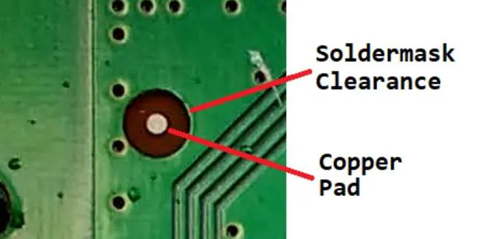
Fiducial marks consist of a solid copper pad, typically circular, exposed without solder mask over the pad itself but with an expanded mask opening for contrast. The standard diameter ranges from 1 mm minimum to 3 mm maximum, ensuring visibility under varying lighting and optics in assembly equipment. A clear zone around the fiducial, free of other copper or components, spans at least 5 mm to prevent optical confusion. Solder mask expansion provides high contrast, with the mask radius often twice the pad radius per IPC-7351 guidelines for land patterns. These dimensions balance detectability with minimal footprint, critical for PCB real estate conservation.
Placement rules dictate positioning fiducials asymmetrically near three corners of the panel, at least 5 mm from edges or v-scoring to avoid clamp interference or damage during depanelization. All fiducials on a panel must match in size and shape to simplify machine calibration, avoiding tolerances exceeding 25 microns between marks. For double-sided assemblies, identical fiducials appear on both sides, aligned vertically. Nonlinear distortions, common in large panels, demand fiducials spaced to encompass the full array, enabling warp compensation. Adhering to these principles upholds IPC-A-600 acceptability criteria for printed boards.
Surface finish uniformity enhances fiducial reliability, as HASL or ENIG provides consistent reflectivity without oxidation. Fiducials reside on outer copper layers, non-plated to maintain planarity. In high-density panels, engineers calculate the effective area consumed, including clearances, which can exceed 100 mm2 per fiducial. These technical constraints directly influence component density limits.
Balancing Accuracy with PCB Real Estate Constraints
High component density amplifies the tension between fiducial precision and available PCB real estate. Larger fiducials offer superior accuracy for fine-pitch devices but consume valuable space better allocated to passives or ICs. Conversely, minimal 1 mm fiducials suffice for coarser placements yet risk detection failures in challenging lighting. SMT design constraints mandate evaluating machine capabilities upfront, as older equipment favors larger marks while modern vision systems handle smaller ones effectively. Space optimization involves simulating fiducial impact on routing density and component count during layout.
Strategic placement minimizes real estate loss by positioning fiducials in panel borders, away from individual board active areas. In dense designs, consolidating global and panel fiducials reduces total count, though this risks over-reliance on fewer references. Clearance zones pose the largest footprint penalty, often dictating minimum board margins. Engineers quantify trade-offs using panel yield models, prioritizing fiducials that maximize assembly CpK values without excessive area sacrifice. J-STD-001 requirements for assembly processes further emphasize robust fiducial design to ensure solder joint integrity.
Panel warpage exacerbates misalignment, where fiducials spaced farther apart provide better correction leverage at the cost of extended clearances. For ultra-dense boards, local fiducials supplement panel ones, distributing references but multiplying space demands. Optimization algorithms in design software can iterate placements to fit within real estate budgets.
Best Practices for Panel Fiducial Implementation
Start with three panel fiducials forming a triangle enclosing the array, placed 5-10 mm from corners for optimal leverage. Use identical 1.5 mm diameter circles for versatility across equipment, with 3 mm solder mask openings and 5 mm copper-free zones. Verify asymmetry to enforce orientation, preventing 180-degree flips. For tab-routed panels, position away from break lines; for v-scored, maintain edge distances per manufacturer specs. Top-side fiducials mirror bottom-side for through-panel alignment.
Incorporate fiducials early in layout to avoid post-hoc shifts disrupting traces. Test detectability with grayscale simulations mimicking machine vision. For high component density, opt for panel-only fiducials if boards share uniform warp profiles, saving intra-board space. Document fiducial coordinates in fabrication files for verification. Regular DFM reviews catch violations like proximity to high-speed signals.
When space is premium, experiment with diamond or filled shapes if circular proves insufficient, though circles remain preferred for isotropy. Pair with tooling holes for mechanical registration, enhancing hybrid alignment. These practices align with IPC-7351, ensuring manufacturability.
Common Challenges and Troubleshooting Insights
Designers often underestimate clearance needs, leading to optical crosstalk where nearby pads confuse cameras. Solution: Enforce 5 mm minimums and review gerbers at 10x zoom. Warped panels amplify errors, mitigated by additional mid-panel fiducials if array exceeds 300 mm. Component density near fiducials risks shadowing; relocate or use locals. Assembly feedback loops reveal tolerances, prompting iterative refinements. Logical auditing preserves accuracy without real estate waste.
Conclusion
Panel fiducial design demands a structured approach to reconcile precision with PCB real estate limitations. By adhering to size, placement, and clearance guidelines, engineers achieve reliable SMT alignment amid rising component density. Strategic space optimization through minimal yet robust fiducials supports high-volume production goals. Integrating these principles early enhances yield and reduces costs. Ultimately, masterful fiducial mark design elevates overall board performance under SMT design constraints.
FAQs
Q1: What key factors define effective fiducial mark design for panels?
A1: Fiducial mark design prioritizes circular copper pads of 1-3 mm diameter with expanded solder mask for contrast and 5 mm clearances. Placement at three asymmetric corners ensures full distortion correction. These elements balance accuracy for high component density while minimizing PCB real estate use. Following IPC-7351 land pattern standards guarantees compatibility across assembly lines.
Q2: How does PCB real estate impact fiducial placement in dense designs?
A2: PCB real estate constraints force minimal fiducial sizes and border placements to free space for components. Clearances dominate area usage, so optimizing to 5 mm suffices for most SMT machines. In high-density panels, panel fiducials alone reduce intra-board needs. This space optimization maintains placement precision without layout compromises.
Q3: What are common SMT design constraints for panel fiducials?
A3: SMT design constraints include edge distances over 5 mm, uniform sizing across the panel, and top-bottom mirroring for double-sided boards. Fiducials must avoid v-cuts and clamps while providing nonlinear warp correction. Component density near fiducials risks errors, so clearances prevent interference. Proper adherence supports sub-25 micron accuracy.
Q4: How to optimize space with fiducials in high component density panels?
A4: Space optimization starts with 1 mm fiducials and triangular panel placements enclosing the array. Consolidate with board globals where possible, enforcing strict clearances. Simulate vision detection to validate minimal designs. This approach preserves PCB real estate for denser packing without sacrificing fiducial mark design integrity.
References
IPC-7351B — Generic Requirements for Surface Mount Design and Land Pattern Standard. IPC
IPC-A-600K — Acceptability of Printed Boards. IPC, 2020
J-STD-001 — Requirements for Soldered Electrical and Electronic Assemblies. IPC


