 ALLPCB


Introduction
PCB silkscreen, also known as the legend layer, plays a crucial role in printed circuit board manufacturing by providing essential markings for identification and assembly. These markings include component designators, polarity indicators, test points, and reference designators that guide technicians during population and troubleshooting. In high-volume production environments, clear silkscreen ensures efficient assembly processes and reduces errors that could lead to field failures. Engineers must prioritize silkscreen design rules to maintain compliance with industry standards and achieve reliable performance. This guide explores key aspects such as PCB silkscreen design rules, silkscreen legibility, silkscreen ink types, silkscreen printing process, and silkscreen alignment, offering factory-driven insights for optimal results. Understanding these elements empowers electric engineers to create boards that meet stringent quality requirements.
What Is PCB Silkscreen and Why It Matters
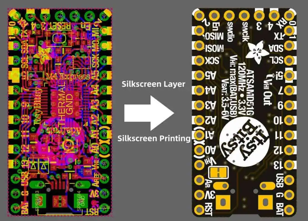
PCB silkscreen refers to the non-conductive ink applied to the surface of a printed circuit board to convey critical information. It typically appears over the solder mask layer and includes text, symbols, logos, and barcodes that aid in manufacturing, assembly, and maintenance. Without proper silkscreen, operators face challenges in identifying components, leading to misplacement or rework during surface-mount technology processes. In complex multilayer boards, silkscreen facilitates automated optical inspection and manual verification, enhancing overall yield. Its importance extends to regulatory compliance, where traceable markings support quality audits and failure analysis. Factory insights reveal that poor silkscreen contributes to up to significant assembly delays, underscoring the need for meticulous design and process control.
Silkscreen must withstand environmental stresses like thermal cycling and chemical exposure encountered in reflow soldering and cleaning. Standards such as IPC-A-600 define acceptability criteria for markings, ensuring legibility post-fabrication. For electric engineers, integrating silkscreen early in the design phase aligns with manufacturability goals and minimizes costly iterations.
PCB Silkscreen Design Rules
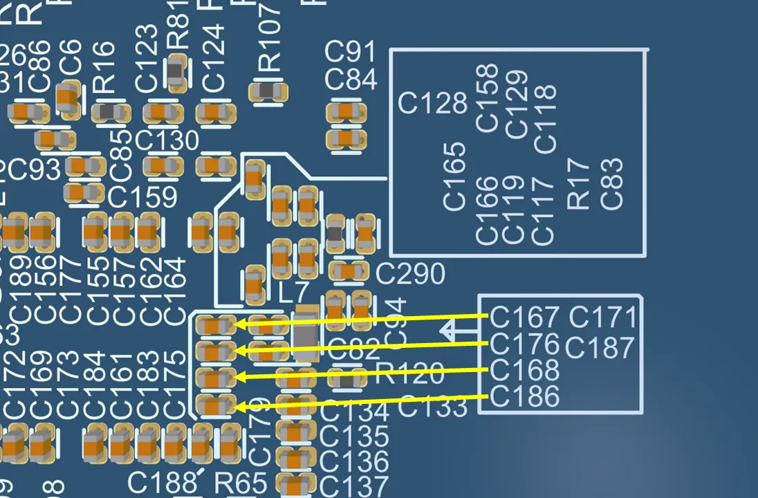
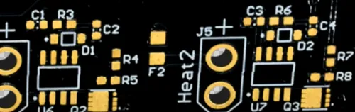
PCB silkscreen design rules establish guidelines for placement, spacing, and feature sizing to ensure manufacturability and functionality. Engineers should avoid overlapping silkscreen with pads, vias, or bare copper to prevent ink bleed or solder mask misalignment during fabrication. Clearances between silkscreen elements and conductive features prevent shorting risks and maintain print fidelity. Line widths and character heights must support the chosen printing method, with thicker strokes improving resolution on fine-pitch boards. Polarization marks for diodes and capacitors require precise positioning relative to component outlines for intuitive assembly.
Adhering to these rules reduces defects like ink cracking or peeling under thermal stress. Factory processes demand fiducial marks near silkscreen areas to aid alignment during printing. Designers benefit from vector-based fonts over raster images to preserve sharpness across scales. Comprehensive rules also account for panelization, where shared edges influence marking placement on production panels.
Ensuring Silkscreen Legibility
Silkscreen legibility is paramount for readable markings that survive handling, soldering, and operational life. High contrast between ink color and solder mask background enhances visibility, with white ink on green mask being a common choice for optimal differentiation. Font selection impacts clarity; sans-serif styles with uniform stroke widths resist blurring during printing. Avoiding overcrowding prevents merging of adjacent characters, which compromises identification during inspection.
IPC-A-600 outlines criteria for marking acceptability, emphasizing durability after exposure to solvents and heat. Legibility testing involves visual inspection under magnification and simulated aging to verify permanence. Engineers should prioritize markings for high-reliability components like power regulators and connectors. In dense layouts, hierarchical labeling prioritizes critical references while relegating secondary info to board edges.
Poor legibility leads to assembly errors, prolonging debug times in prototypes. Factory-driven practices include matte finishes to reduce glare under LED lighting in cleanrooms.
Silkscreen Ink Types
Silkscreen ink types vary by chemistry and application method, each offering trade-offs in adhesion, durability, and process compatibility. Epoxy-based inks provide robust mechanical strength and chemical resistance, making them suitable for traditional screen printing on rigid boards. UV-curable inks cure rapidly under ultraviolet light, enabling higher throughput in volume production while maintaining flexibility on flex circuits. Liquid photoimageable inks allow fine-line definition through exposure and development, ideal for high-density interconnects.
Non-conductive formulations prevent electrical interference, with pigmentation ensuring opacity for legibility. Acrylic inks offer cost-effective alternatives for less demanding applications, balancing performance and price. IPC-4781 specifies qualification tests for inks, covering adhesion, abrasion resistance, and thermal stability. Selection depends on board finish, such as HASL or ENIG, to ensure compatibility without delamination.
Thicker ink layers enhance durability but may increase cure times. Factory insights favor dual-cure systems combining thermal and UV for hybrid performance.
The Silkscreen Printing Process
The silkscreen printing process begins with artwork preparation, converting design files into stencil patterns for ink deposition. Traditional screen printing uses a mesh screen coated with emulsion, exposed to UV light to form openings corresponding to markings. A squeegee forces ink through the stencil onto the PCB surface, followed by drying or curing to fix the image. This method excels in high-volume runs due to its speed and cost-efficiency.
Liquid photoimageable (LPI) processes apply ink as a liquid film, pattern it photolithographically, and develop unexposed areas for precise features. Direct legend printing (DLP) employs inkjet technology to jet droplets directly from digital data, eliminating stencils for prototyping flexibility. Each step requires precise registration to align with underlying layers, using fiducials for machine vision.
Post-print inspection verifies coverage and defects before oven curing. Process controls like viscosity monitoring ensure consistent ink flow. IPC-6012 performance specs validate silkscreen integrity after reflow simulation.
Mastering Silkscreen Alignment
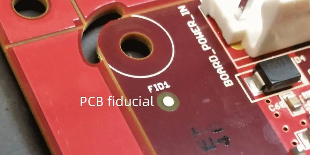
Silkscreen alignment ensures markings register accurately with board features, preventing offset that obscures references. Fiducial marks, global and local, provide reference points for automated alignment systems during printing. Panel-level alignment compensates for substrate warpage, critical in large production panels. Engineers specify fiducials in corners and near dense silkscreen zones to minimize errors.
Misalignment arises from screen tension variations or board movement, addressed by vacuum hold-downs and optical feedback. Tolerances tighten for Class 3 boards, demanding sub-mil precision. Factory alignment verification uses automated optical character recognition to flag deviations.
Proper alignment supports downstream processes like stencil printing for solder paste. Iterative design reviews incorporate feedback from pilot runs.
Best Practices for PCB Silkscreen
Implement best practices by integrating silkscreen planning during schematic capture, using dedicated layers in CAD software. Simulate printability with Gerber viewers to detect overlaps early. Select ink and process based on board complexity; LPI for fine pitch, epoxy screen for standard. Standardize colors across product families for supply chain efficiency.
Conduct design for manufacturability reviews focusing on silkscreen density and edge proximity. Test prototypes under accelerated aging to validate legibility. Collaborate with fabricators for process-specific rules.
Document revisions clearly on silkscreen to track iterations. These practices align with IPC standards, boosting yield and reliability.
Conclusion
Mastering PCB silkscreen demands attention to design rules, legibility, ink selection, printing processes, and alignment for effective markings. Factory-driven adherence to standards like IPC-A-600 and IPC-4781 ensures durable, readable boards that streamline assembly and maintenance. Electric engineers benefit from proactive integration of these elements, reducing defects and enhancing product longevity. Prioritizing silkscreen elevates overall PCB quality, supporting reliable performance in demanding applications.
FAQs
Q1: What are key PCB silkscreen design rules for electric engineers?
Q1: PCB silkscreen design rules emphasize clearances from pads and vias, adequate line widths, and strategic placement to avoid overlaps. Maintain sufficient spacing for ink flow during printing and ensure compatibility with assembly processes. Following these rules per IPC guidelines prevents defects and supports high-yield manufacturing. Engineers should verify rules against board class for optimal results.
Q2: How can silkscreen legibility be improved on dense PCBs?
A2: Silkscreen legibility improves with high-contrast inks, bold fonts, and hierarchical labeling prioritizing critical marks. Avoid overcrowding by using abbreviations where possible and matte finishes to reduce glare. Standards like IPC-A-600 guide minimum requirements for readability post-processing. Prototype testing under various lighting confirms effectiveness.
Q3: What are common silkscreen ink types and their uses?
A3: Common silkscreen ink types include epoxy for durability, UV-curable for speed, and liquid photoimageable for precision. Epoxy suits rigid boards with thermal exposure, while LPI excels in fine features. IPC-4781 qualifies inks for adhesion and resistance. Selection matches process and environment for longevity.
Q4: Why is silkscreen alignment critical in PCB manufacturing?
A4: Silkscreen alignment ensures markings match component positions, aiding assembly and inspection. Fiducials enable precise registration, compensating for panel distortions. Poor alignment causes misreads and rework. Automated systems verify tolerances, aligning with performance specs in IPC-6012.
References
IPC-A-600K — Acceptability of Printed Boards. IPC, 2020
IPC-4781 — Qualification and Performance Specification for Printed Board Legend Inks. IPC
IPC-6012E — Qualification and Performance Specification for Rigid Printed Boards. IPC, 2017


