 ALLPCB


Introduction
The electronics industry has fully embraced lead-free solder to comply with environmental regulations and enhance sustainability in manufacturing processes. In high-frequency circuits, including RF and microwave applications, the transition introduces unique challenges related to lead-free solder high-frequency performance and lead-free solder signal integrity. Engineers must address how these solders interact with transmission lines, impedance control, and overall circuit reliability. Poorly managed solder joints can degrade signals through increased losses or mismatches, compromising system performance. This article explores the principles behind these effects and provides practical strategies for optimization. By understanding the material behaviors and assembly techniques, designers can achieve robust high-speed boards.
Lead-free solders, primarily tin-silver-copper alloys, replaced traditional tin-lead options to reduce hazardous waste and meet global standards. Their higher melting points demand elevated reflow temperatures, which stress PCB materials and components during assembly. In high-frequency environments above several gigahertz, signal paths behave as transmission lines where even minor joint imperfections amplify attenuation or reflections. Lead-free solder signal integrity becomes critical because joint microstructure influences electrical conductivity and mechanical stability under thermal cycling. For RF applications, consistent impedance matching prevents power loss and distortion. Microwave circuits, operating at even higher frequencies, amplify these concerns, making solder selection and process control essential for maintaining low insertion loss.
Engineers designing for telecommunications, radar, or 5G infrastructure face amplified risks from solder-related anomalies. Voids or uneven fillets alter local capacitance and inductance, disrupting controlled impedance traces. The stiffer nature of lead-free alloys also affects vibration resistance in deployed systems. Without optimization, these factors lead to bit errors, reduced range, or outright failures. Industry standards like IPC J-STD-001 outline requirements for soldered assemblies to ensure quality across lead-free processes. Proactive management translates to longer service life and compliance in demanding sectors.
Why Lead-Free Solder Matters in High-Frequency Circuits
Lead-free solders, primarily tin-silver-copper alloys, replaced traditional tin-lead options to reduce hazardous waste and meet global standards. Their higher melting points demand elevated reflow temperatures, which stress PCB materials and components during assembly. In high-frequency environments above several gigahertz, signal paths behave as transmission lines where even minor joint imperfections amplify attenuation or reflections. Lead-free solder signal integrity becomes critical because joint microstructure influences electrical conductivity and mechanical stability under thermal cycling. For RF applications, consistent impedance matching prevents power loss and distortion. Microwave circuits, operating at even higher frequencies, amplify these concerns, making solder selection and process control essential for maintaining low insertion loss.
Engineers designing for telecommunications, radar, or 5G infrastructure face amplified risks from solder-related anomalies. Voids or uneven fillets alter local capacitance and inductance, disrupting controlled impedance traces. The stiffer nature of lead-free alloys also affects vibration resistance in deployed systems. Without optimization, these factors lead to bit errors, reduced range, or outright failures. Industry standards like IPC J-STD-001 outline requirements for soldered assemblies to ensure quality across lead-free processes. Proactive management translates to longer service life and compliance in demanding sectors.
Technical Principles of Lead-Free Solder in High-Frequency Performance
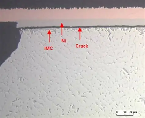
Lead-free solders form distinct intermetallic compounds (IMCs) at the interfaces with copper pads and component leads, such as Cu6Sn5 layers that grow thicker over time compared to leaded joints. This growth modifies the joint's electrical properties, potentially increasing series resistance in signal paths at high frequencies where skin effect confines currents to surfaces. In lead-free solder RF applications, rougher joint surfaces from incomplete wetting exacerbate dielectric losses and radiation. Signal propagation relies on uniform conductor geometry, but solder fillet variations introduce discontinuities that reflect energy back toward the source. At microwave frequencies, these reflections compound, degrading return loss metrics.
Thermal expansion mismatches between solder, PCB laminate, and components heighten risks during reflow, leading to warpage that misaligns traces and vias. Warped boards disrupt stripline or microstrip geometries, altering characteristic impedance and causing crosstalk between adjacent signals. Lead-free alloys exhibit higher stiffness, reducing compliance and increasing fatigue crack propagation under operational stresses. Grain structure in the bulk solder influences phonon scattering, subtly raising resistivity at elevated frequencies. Engineers must model these effects using field solvers to predict lead-free solder impedance matching behavior. JEDEC J-STD-020 classifies components for moisture sensitivity, guiding reflow profiles to minimize voids that trap air and create high-impedance spots.
Electromagnetic coupling through solder bridges or excess volume further complicates high-frequency behavior. In dense layouts, proximity effects demand precise solder deposition to avoid shorting grounds or signals. Surface finish on pads, like ENIG or OSP, interacts differently with lead-free flux, affecting IMC uniformity and thus high-frequency attenuation. These principles underscore the need for holistic design consideration beyond just DC performance.
Challenges in Signal Integrity and Impedance Control
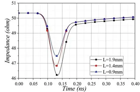
Maintaining lead-free solder signal integrity requires vigilance against reflow-induced defects that manifest as time-domain reflectometry (TDR) anomalies. Excessive IMC thickness reduces joint conductivity, manifesting as insertion loss spikes beyond 10 GHz. Impedance mismatches at solder-to-trace transitions arise from varying solder height, which shifts effective dielectric loading. In multilayer boards, via-in-pad designs amplify these issues if solder wicks unevenly, creating stubs that resonate at unwanted frequencies. Microwave circuits suffer most, as phase shifts from joint losses distort modulation schemes.
Crosstalk escalates when solder fillets bridge signal and ground planes, shorting return paths and injecting noise. Lead-free pastes often yield smaller standoff heights, compressing components closer to the board and intensifying parasitic capacitance. Reliability testing reveals accelerated aging in high-frequency joints due to electromigration, where current densities crowd at IMC boundaries. Troubleshooting involves cross-section analysis to quantify void percentages and fillet concavity. Optimizing flux chemistry mitigates oxidation, promoting better wetting for smoother transitions.
Best Practices for Optimizing Lead-Free Solder in RF and Microwave Circuits
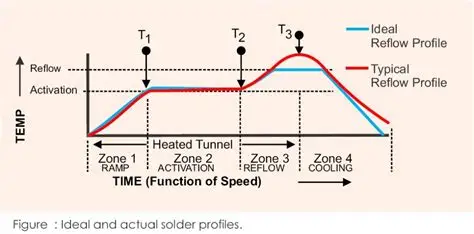
Select solder pastes with fine particle sizes for uniform deposition in fine-pitch components common to RF boards. Type 4 or finer powders reduce viscosity, enabling precise volume control to preserve lead-free solder impedance matching. Implement nitrogen atmospheres during reflow to suppress oxidation and refine grain structure, lowering bulk resistivity. Profile the oven to achieve liquidus times compliant with component ratings, avoiding prolonged exposure that thickens IMCs.
Pad design plays a pivotal role: enlarge solder mask-defined pads slightly to accommodate fillet spread without encroaching on adjacent traces. For microstrip lines, bevel edges to minimize solder climb, maintaining 50-ohm or 100-ohm differentials. In lead-free solder microwave circuits, embed vias with back-drilling to eliminate stubs, and fence ground vias around high-speed signals for shielding. Post-reflow inspection using automated optical systems verifies fillet symmetry per IPC J-STD-001 criteria, catching defects early.
Layer stackup optimization integrates low-loss dielectrics with lead-free compatible resins that resist delamination. Simulate solder volume effects on impedance using 3D solvers before fabrication. For assembly, stencil apertures at 100-120% of pad area prevent bridging while ensuring heel formation. Thermal profiling with thermocouples on test coupons validates process windows. These practices collectively enhance lead-free solder high-frequency performance, yielding boards with <1 dB loss per inch at mmWave bands.
Troubleshooting Common Issues in High-Frequency Assemblies
Engineers often encounter head-in-pillow defects where the solder ball fails to fully merge with the paste deposit, creating soft joints prone to high-frequency fatigue. Root causes include mismatched reflow ramps or paste oxidation; solutions involve flux activators tuned for lead-free alloys. Tombstoning in chip components disrupts ground planes, altering impedance; mitigate with symmetric thermal mass and hold times above liquidus.
Excessive voids from outgassing signal as high-resistance paths in TDR scans; vacuum-assisted reflow or low-residue fluxes resolve this. In RF applications, electromigration manifests as intermittent opens after burn-in; select low-alpha alloys to curb this. Cross-reference assembly data with electrical tests to correlate defects with performance drops. Iterative process tweaks, grounded in standards, restore integrity.
Conclusion
Lead-free solder enables sustainable high-frequency circuits but demands meticulous attention to joint quality for optimal lead-free solder high-frequency performance and signal integrity. Key principles like IMC control and reflow optimization directly impact impedance matching and loss in RF and microwave designs. Best practices in paste selection, pad geometry, and profiling ensure reliable assemblies. By adhering to established guidelines, engineers minimize risks and maximize throughput. Future advancements in alloy compositions promise further improvements, but current techniques suffice for demanding applications. Prioritizing these strategies delivers robust, high-performing boards.
FAQs
Q1: How does lead-free solder affect signal integrity in high-frequency PCBs?
A1: Lead-free solders introduce higher reflow temperatures that can cause warpage and uneven joints, leading to reflections and losses. Thicker IMCs increase resistance, impacting skin effect at GHz frequencies. Optimized profiles and pad designs maintain clean waveforms. Troubleshooting with TDR identifies mismatches early. This ensures reliable lead-free solder signal integrity without compromising speed.
Q2: What are best practices for lead-free solder impedance matching in RF applications?
A2: Use controlled solder volumes via precise stencils to avoid altering trace geometry. Simulate joint effects on characteristic impedance pre-layout. Employ low-loss laminates compatible with lead-free processes. Ground stitching vias enhance return paths. These steps preserve 50-ohm matching for lead-free solder RF applications, minimizing VSWR.
Q3: Why is lead-free solder challenging for microwave circuits?
A3: Microwave frequencies amplify joint discontinuities, where rough surfaces and voids cause excessive attenuation. Stiffer alloys fatigue faster under vibration. Reflow optimization per JEDEC J-STD-020 prevents delamination. Fine-pitch handling demands advanced inspection. Proper execution upholds lead-free solder microwave circuits performance.
Q4: How to optimize lead-free solder high-frequency performance during assembly?
A5: Profile reflow for minimal liquidus time to control IMC growth. Nitrogen purging improves wetting. Verify fillets against IPC J-STD-001. Test signal loss post-assembly. These ensure low insertion loss and high reliability in demanding environments.
References
IPC J-STD-001G — Requirements for Soldered Electrical and Electronic Assemblies. IPC, 2017
JEDEC J-STD-020E — Moisture/Reflow Sensitivity Classification for Nonhermetic Solid State Surface Mount Devices. JEDEC, 2014
IPC-6012E — Qualification and Performance Specification for Rigid Printed Boards. IPC, 2017


