ALLPCB


Overview
This article discusses the application of LDMOS in ESD design. LDMOS is a power semiconductor device mainly used in high-voltage applications. For ESD protection of high-voltage chips, a GGNLDMOS-based design approach can be adopted.
Basic Operating Principle of LDMOS
Before explaining the ESD protection mechanism, a brief summary of the LDMOS operating principle is given.
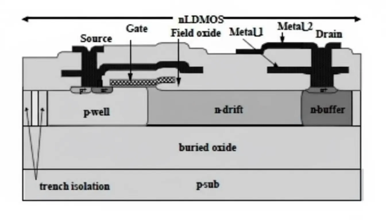
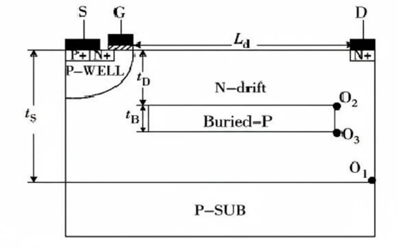
To improve voltage withstand, N-LDMOS forms an N-drift region. To increase the gate voltage tolerance, the gate above the N-drift is placed over field oxide, using the field oxide as the dielectric. Because of this design, the NLDMOS device has high negative VGD and VSD withstand voltages (V: D→G, D→S).
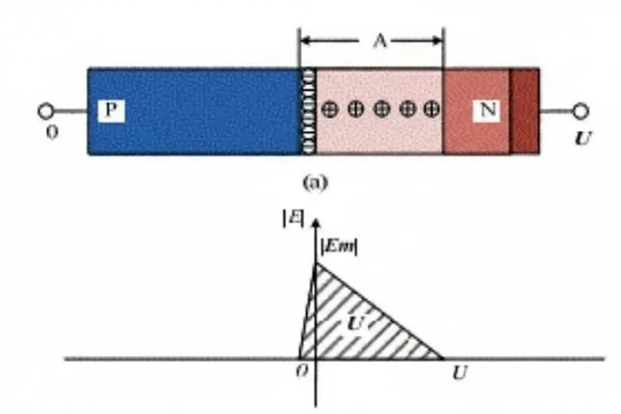
The doping concentration of the N-drift well is lower than that of the p-well and n-buffer. Its contact with the p-well forms a space charge region. For a graded junction with concentration difference, the space charge region will mainly distribute within the N-drift, as shown.
When the device is off, this space charge region is equivalent to embedding a high-voltage "resistor" in the NLDMOS. This "resistor" allows the drain to withstand high voltage. When the gate is turned on, the gate above the p-well forms a channel as in a normal MOS, while the gate above the N-drift creates an accumulation layer near the field oxide, forming a channel. The gate voltage effectively pushes the space charge region into the device, forming a "channel" under the field oxide.
Techniques to Improve High-Voltage Performance
To pursue higher voltage tolerance, more techniques are applied to LDMOS design. Common approaches include RESURF, field plates, and super junction.
Because NLDMOS voltage capability also determines its ESD device voltage limit, the following briefly introduces these three designs.
RESURF
RESURF implants a P-buried layer into the N-drift, enlarging the space charge distribution in the N-drift, modulating the electric field distribution, and changing the reverse breakdown node.
Field Plates
Field plates are the M1 and M2 metal layers above the drain; the metal extends over the gate to form the field plate. Field plates suppress surface electric field concentration by altering surface potential distribution, producing a more uniform surface field and improving breakdown voltage.
Field plates mitigate electric field crowding at the metallurgical junction, reducing the peak field at the junction while introducing a new peak at the field plate edge, which increases overall voltage capability.
Super Junction
Super junction is widely used for ultra-high-voltage devices and is an extension of the RESURF technique. It creates deep, alternating wells to increase device breakdown voltage.
Current super junction processes can provide 600 V to 1000 V ratings, but they also introduce several process and reliability challenges.
ESD Protection Strategies in High-Voltage BiCMOS
LDMOS is often used in industrial-grade applications where operating environments are more complex and ESD and surge requirements are higher. Therefore, high-voltage ESD design is more challenging.
In high-voltage BiCMOS processes, there are two ESD protection strategies: stacking low-voltage devices, or using dedicated high-voltage ESD protection devices. Stacking requires larger area but has smaller process variation. High-voltage protection devices require less area but have larger process variation and a higher risk of latch-up.
Either approach requires custom ESD devices, and the foundry provides corresponding ESD design rules. The typical LDMOS connection for ESD protection is shown below.
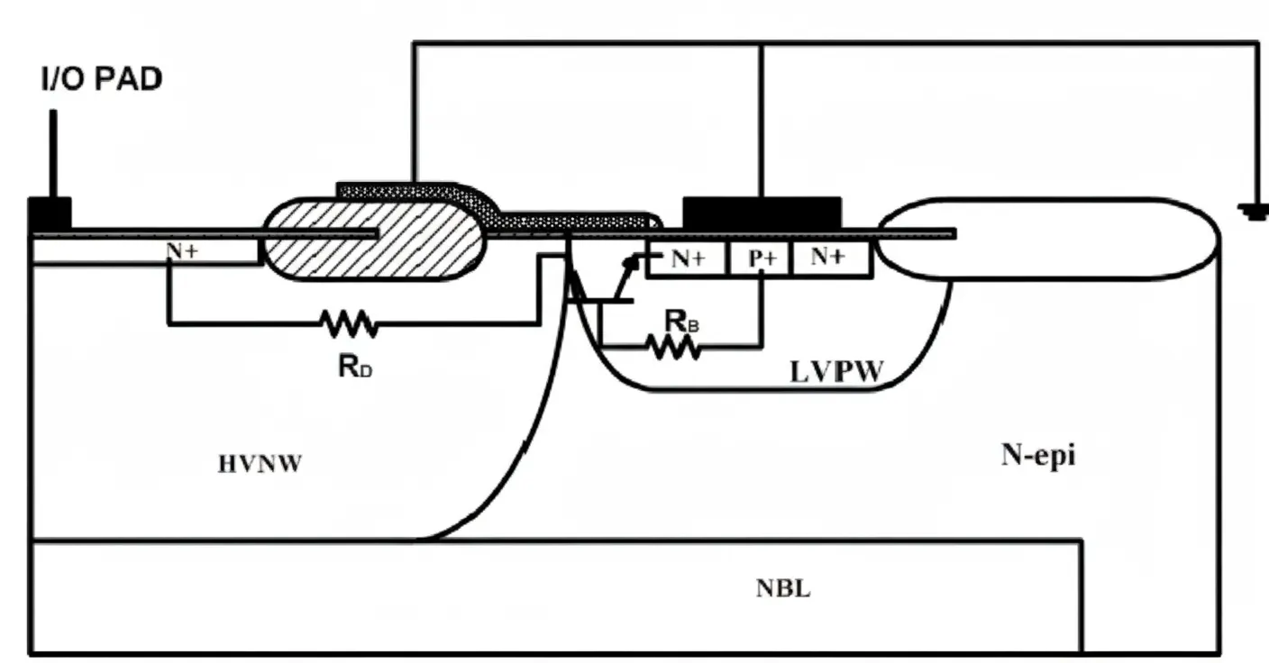
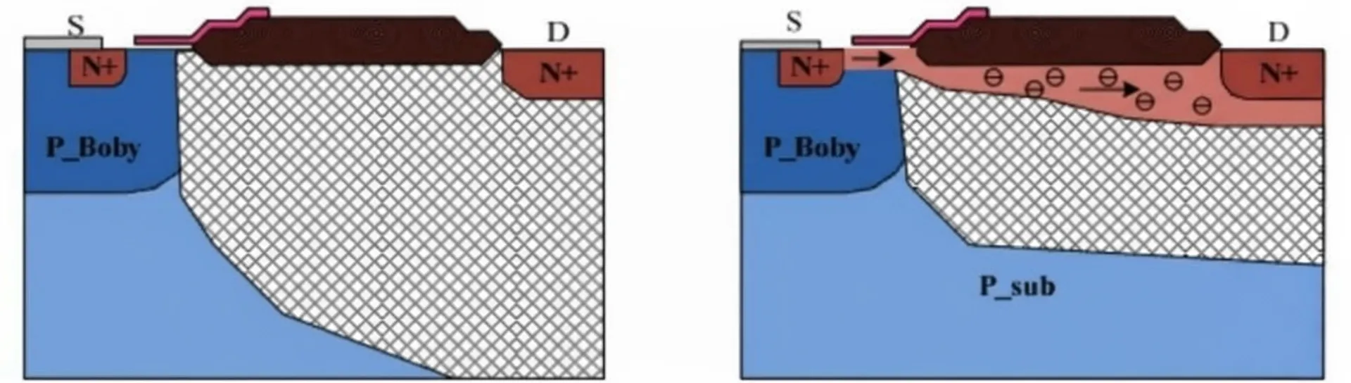
Similar to GGN MOS, GGNLDMOS ties source, gate, and body to ground, with the drain connected to the I/O pad. Because LDMOS has a drift region and a larger drain area, its drain withstand voltage and internal breakdown voltage are higher; trigger and holding voltages are also relatively high. Given these characteristics, major layout changes are often unnecessary; focus should be placed on device isolation.
Challenges: Thermal and Field Concentration
Some foundries do not recommend GGNLDMOS mainly due to thermo-electric concerns. LDMOS has a higher risk of thermal failure: excessive electric field at metallurgical junctions concentrates heat and can cause soft failures. Therefore, GGNLDMOS design must prevent field crowding and redistribute the electric field.
Two main approaches to improve field distribution are changing layout dimensions and modifying device structure.
Layout Dimensions
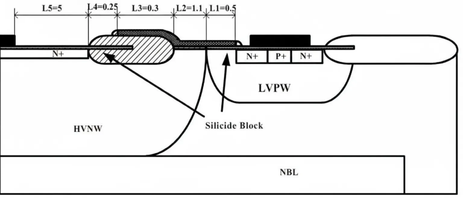
L1 is the distance from the gate to above the P-well. L2 is the distance the thick gate oxide spans over the N-well. L3 is gate length. L4 is the ungated drift region length. L5 is the distance between the N-implant and the contact. Adjusting L4 and L3 changes device breakdown voltage. Shortening L5 and L1 can improve current conduction while increasing breakdown voltage, helping to prevent junction overheating and device damage.
Device Structure
To improve GGNLDMOS ESD robustness, introduce graded junctions between wells, i.e., change the well structure. Where DRC permits, nest an NWELL inside an HNWELL to create a concentration gradient. This reduces carrier concentration at a single junction and helps mitigate thermo-electric effects.