ALLPCB


Introduction
High-frequency PCB design requires precise management of signal integrity, and PCB impedance control forms a core element of that process. Engineers specify target impedance values for critical traces to minimize reflections and maintain consistent signal propagation. Inner layer copper thickness directly influences the geometry of transmission lines, affecting the characteristic impedance in both stripline and microstrip configurations. Variations in copper thickness during manufacturing can shift impedance outside acceptable tolerances, leading to performance issues in applications such as telecommunications and data transmission equipment. Understanding this relationship allows designers to incorporate appropriate margins during stackup planning and trace sizing.
What Is PCB Impedance Control and Why It Matters
PCB impedance control refers to the practice of designing and manufacturing printed circuit boards so that specific traces exhibit a predetermined characteristic impedance, typically 50 ohms or 100 ohms for differential pairs. In high-frequency PCB design, this control prevents signal distortion that arises when impedance mismatches occur along the transmission path. Copper thickness impedance effects become particularly noticeable in inner layers, where the conductor forms part of a symmetric stripline structure surrounded by dielectric material on both sides. Without proper control, even small deviations in copper thickness can alter the effective trace width and height, changing the inductance and capacitance per unit length. This matters for engineers working on high-speed digital or RF circuits, where maintaining signal integrity directly impacts overall system reliability and data rates.
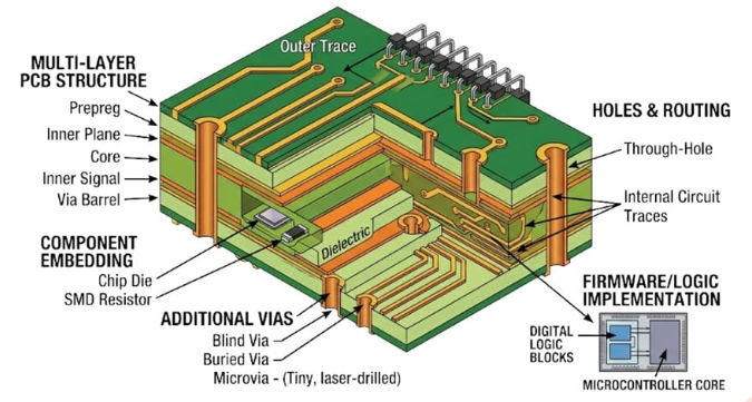
Technical Principles: Mechanisms Linking Copper Thickness to Transmission Line Impedance
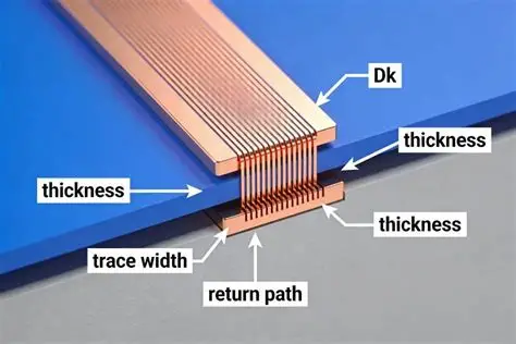
The characteristic impedance of a transmission line depends on the ratio of inductance to capacitance along the conductor, both of which vary with physical dimensions. In inner layer constructions, increased copper thickness raises the trace height, which modifies the electromagnetic field distribution and typically lowers the impedance for a fixed trace width. Conversely, thinner copper increases impedance because the reduced conductor cross-section alters the current distribution and fringing fields. These effects interact with dielectric constant, trace width, and spacing to the reference planes, creating a multivariable relationship that designers model using electromagnetic simulation tools. Manufacturing processes introduce tolerances on copper thickness, usually expressed as a percentage of nominal value, which must be accounted for when calculating final impedance. IPC-6012E outlines qualification requirements for rigid printed boards, including considerations for conductor thickness that support consistent impedance performance.
Practical Solutions and Best Practices
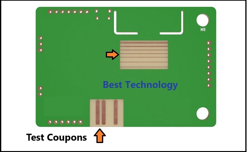
Designers begin by selecting copper weights that balance electrical performance with manufacturability, often starting with 0.5 oz or 1 oz copper for inner layers in high-frequency applications. They then adjust trace widths iteratively using impedance calculators or field solvers while incorporating expected thickness tolerances from the fabrication process. Stackup symmetry and dielectric material selection further stabilize impedance by minimizing variations in the surrounding environment. During layout, engineers specify controlled impedance PCB requirements on fabrication drawings, including target values, tolerance bands, and test coupon locations for verification. Collaboration between design and manufacturing teams helps align copper thickness targets with achievable process capabilities, reducing the need for post-fabrication adjustments. IPC-A-600K provides acceptability criteria for printed boards that include conductor thickness evaluation, supporting quality verification of impedance-controlled designs.
Manufacturing and Design Integration Insights
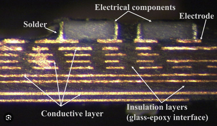
Fabrication sequences such as pattern plating or foil construction influence the final copper thickness distribution across inner layers, with potential for localized variations that affect impedance uniformity. Engineers address this by specifying minimum and maximum copper thickness limits in addition to nominal values, allowing fabricators to optimize processes accordingly. Test structures incorporated into production panels enable direct impedance measurement using time-domain reflectometry or vector network analyzers, confirming that the finished board meets specifications. When discrepancies arise, root-cause analysis often traces back to copper thickness deviations, prompting refinements in etching or plating parameters. These steps ensure that high-frequency PCB designs translate reliably from simulation to physical hardware.
Conclusion
Inner layer copper thickness represents a critical variable in achieving reliable PCB impedance control for high-frequency applications. By understanding its impact on transmission line impedance and incorporating appropriate design margins, engineers can produce boards that maintain signal integrity across operating conditions. Structured attention to stackup definition, tolerance analysis, and verification methods supports consistent results without unnecessary complexity. Adherence to established industry practices further strengthens the link between design intent and manufactured performance.
FAQs
Q1: How does copper thickness affect PCB impedance control in high-frequency designs?
A1: Copper thickness modifies the conductor height in inner layer transmission lines, directly influencing the inductance and capacitance that determine characteristic impedance. Thicker copper generally decreases impedance for a given trace width, while thinner copper increases it. Designers account for this relationship during trace sizing and stackup planning to meet target values in controlled impedance PCB layouts. Manufacturing tolerances on copper thickness must be considered to keep final impedance within specification.
Q2: What role does inner layer copper thickness play in high-frequency PCB design?
A2: Inner layer copper thickness contributes to the overall geometry of stripline or embedded microstrip structures, affecting electromagnetic field confinement and impedance consistency. In high-frequency PCB design, even modest thickness variations can shift impedance outside acceptable ranges, impacting signal integrity. Proper specification of copper weight and tolerance during the design phase helps maintain transmission line impedance performance throughout the board.
Q3: Why is controlled impedance PCB important when copper thickness varies?
A3: Variations in copper thickness alter the effective dimensions of signal traces, changing the impedance profile along high-speed paths. Controlled impedance PCB techniques compensate for these variations through adjusted trace widths, dielectric spacing, and verification testing. This approach ensures reliable signal propagation in high-frequency applications despite normal manufacturing differences in conductor thickness.
Q4: How can engineers manage copper thickness impedance effects during design?
A4: Engineers manage copper thickness impedance effects by modeling multiple thickness scenarios in simulation tools and selecting trace dimensions that remain within tolerance across the expected range. They also define clear requirements for copper weight and uniformity on fabrication drawings. This proactive approach supports consistent transmission line impedance in the finished high-frequency PCB.
References
IPC-6012E — Qualification and Performance Specification for Rigid Printed Boards. IPC, 2017
IPC-A-600K — Acceptability of Printed Boards. IPC, 2020