ALLPCB


Introduction
Silkscreen layers on printed circuit boards provide an essential opportunity to enhance both functionality and aesthetics. Engineers often overlook the potential of silkscreen graphics and logos to elevate a PCB from a mere functional component to a branded, professional product. Adding logos to PCB silkscreen allows companies to imprint their identity directly onto the board, fostering recognition in prototypes, production runs, and end-user applications. Beyond branding, these elements aid in assembly, testing, and troubleshooting by clearly marking reference designators, polarity indicators, and custom graphics. For electric engineers designing complex circuits, adhering to silkscreen graphic design guidelines ensures reliability and manufacturability. This article explores practical strategies to integrate company logos on PCBs effectively, drawing on industry-established practices.
What Is PCB Silkscreen and Why Does It Matter?
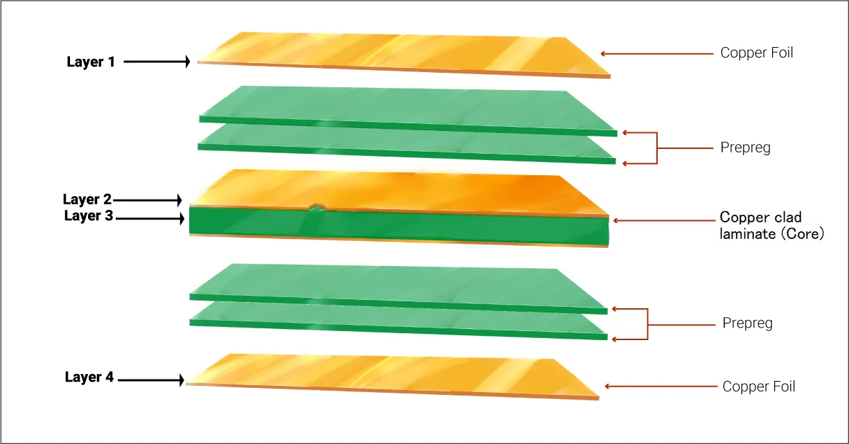
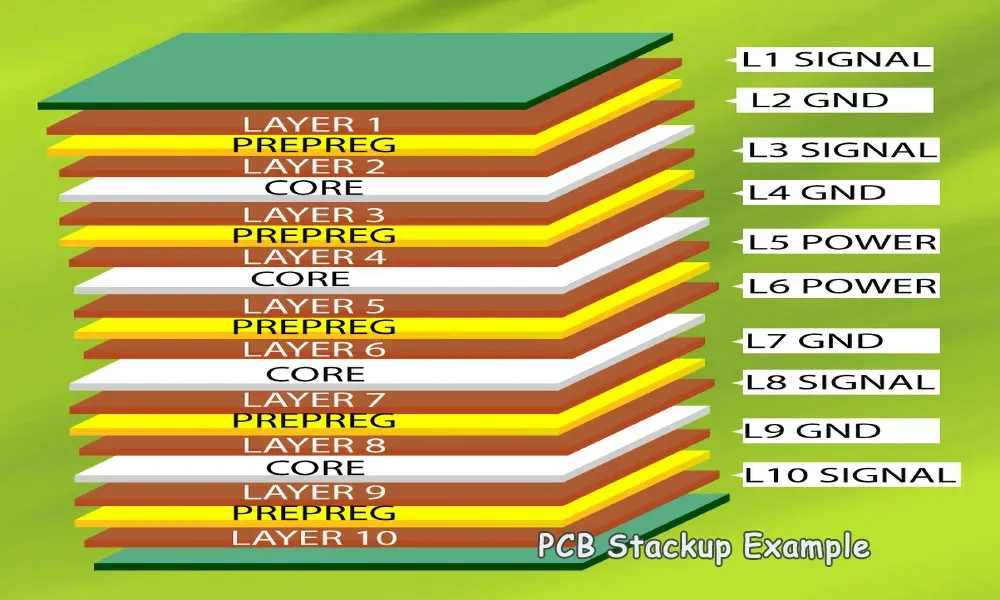
PCB silkscreen, also known as the legend or nomenclature layer, consists of printed ink applied to the board's surface, typically over the solder mask. This layer carries alphanumeric characters, symbols, lines, and graphics that convey critical information without interfering with electrical performance. In manufacturing, silkscreen is one of the final steps after etching and solder mask application, using screen-printing techniques to deposit durable epoxy-based inks. Its primary roles include component identification, board versioning, and safety warnings, all of which streamline production and field service.
The relevance of silkscreen extends to professional presentation, particularly for electric engineers presenting prototypes to stakeholders. A well-executed company logo on PCB not only reinforces brand identity but also signals attention to detail in design and fabrication. Poorly designed silkscreen can lead to misassembly or inspection failures, while optimized graphics improve traceability throughout the product lifecycle. In high-volume production, these markings facilitate automated optical inspection and manual verification, reducing errors. Ultimately, silkscreen bridges the gap between engineering functionality and commercial appeal.
Technical Principles of Silkscreen Graphics
Silkscreen graphics rely on precise ink deposition to achieve sharp edges and consistent opacity. The process begins with artwork preparation in PCB design software, where vector-based elements ensure scalability without pixelation. Ink adhesion to the solder mask requires compatible chemistries, typically matte white or yellow epoxy inks cured via UV or thermal methods for abrasion resistance. Contrast against the underlying green or black solder mask is crucial for visibility under various lighting conditions during assembly.
Line widths and spacings must accommodate screen-printing tolerances, preventing bridging or voids that compromise legibility. Fonts should feature uniform stroke widths to avoid thinning during printing, with sans-serif styles preferred for clarity at reduced sizes. Graphics like logos demand simplification to eliminate fine details that blur under ink spread. Electric engineers must consider board warpage or flexing, as these can distort markings over time, emphasizing the need for flexible ink formulations.
Adherence to IPC-A-600 standards ensures markings meet acceptability criteria for class 2 and class 3 boards, focusing on legibility post-fabrication. These guidelines address defects such as ink peeling or incomplete fills, which are common failure modes. By understanding these principles, designers can create graphics that withstand environmental stresses like humidity and handling.
Silkscreen Graphic Design Guidelines for Optimal Results
Effective silkscreen graphic design guidelines start with placement strategies to avoid interference with active areas. Keep markings at least a safe distance from exposed copper pads, vias, and fiducials to prevent solder wicking or contamination during reflow. Orient text and logos parallel to board edges for easier reading, and reserve the top side for primary graphics while using the bottom for secondary information if needed. Multi-layer boards benefit from silkscreen on both sides, but alignment during stacking prevents overlap shadows.
Color selection influences durability and visibility; white ink offers high contrast on dark masks, while custom colors require additional screening passes that increase costs. Monochrome designs simplify production, as multi-color silkscreen demands precise registration between layers. Test graphics for scalability by simulating print resolutions, ensuring elements remain distinct at fabrication scales.
Silkscreen graphic design guidelines also emphasize hierarchy: prioritize reference designators near components, followed by version numbers and logos in open areas. Avoid enclosing graphics within tight boundaries that limit ink flow. For electric engineers, vector formats like Gerber apertures facilitate direct transfer to manufacturing, minimizing interpretation errors.
IPC-4781 provides qualification protocols for legend inks, verifying adhesion, solvent resistance, and color fastness through standardized tests. These ensure graphics endure assembly processes like wave soldering or conformal coating.
Best Practices for Adding Logos to PCB Silkscreen
Adding logos to PCB silkscreen begins with preparing artwork in a suitable format. Convert company logos to monochrome vector outlines, removing gradients, shadows, or halftones that do not reproduce well in ink. Simplify complex shapes by merging paths and increasing stroke widths to match printing capabilities. Electric engineers should verify logo dimensions against board real estate, scaling proportionally to fit non-critical zones like edges or corners.
Position the logo strategically: central areas draw attention but risk obscuring traces, while borders provide prominence without functional impact. Mirror images for bottom-side placement if double-sided silkscreen is used, accounting for board flip during inspection. Include a negative space buffer around the logo to enhance definition and prevent bleed into adjacent features.
During design review, perform design rule checks for silkscreen overlaps with solder mask openings. Collaborate with fabricators early to confirm ink compatibility and panelization effects on logo alignment in arrays. Prototyping reveals issues like ink cracking on flexible regions, allowing iterations before full production.
Company logo on PCB integration elevates prototypes for investor demos or customer samples, signaling production readiness. Track revisions by pairing logos with date codes in silkscreen, aiding inventory management.
Manufacturing Considerations for Silkscreen Durability
In PCB fabrication, silkscreen application follows solder mask curing, using emulsion screens stretched over frames with photo-imaged stencils. Ink is squeegeed through apertures onto the board, then cured to form a robust layer resistant to solvents and mechanical wear. Dry film or liquid photoimageable legends offer finer resolution for intricate graphics but demand controlled environments to avoid defects.
Durability testing simulates end-use conditions, checking for fade resistance under UV exposure or abrasion from handling. Electric engineers specify class levels per IPC-6012, influencing ink thickness and cure profiles. Multi-color logos require sequential printing with alignment marks, increasing cycle times but enabling branded differentiation.
Panel-level processing affects logo consistency; array borders may show edge effects, so centralize critical graphics. Post-print inspection via automated systems verifies fill completeness and registration, rejecting boards with voids larger than allowable limits.
Common Pitfalls in Silkscreen Logos and How to Avoid Them
One frequent issue in adding logos to PCB silkscreen is insufficient line thickness, leading to feathering or disappearance of fine details post-print. Designers counter this by outlining paths with adequate width and previewing at 1:1 scale. Overcrowded layouts cause ink bridging between elements, resolved by enforcing clearances in design rules.
Poor contrast on non-standard solder masks hampers readability; test swatches confirm visibility before commitment. Logos spanning bend areas on rigid-flex boards crack under flexure, mitigated by segmented designs or omission. Thermal expansion mismatches during reflow can shift silkscreen relative to features, addressed by low-shrinkage inks qualified per standards.
Assembly processes exacerbate issues: legend ink dissolving in fluxes requires solvent-resistant formulations. Troubleshooting involves root-cause analysis, such as screen tension inconsistencies causing uneven deposition. Electric engineers mitigate risks through iterative prototyping and fabricator feedback loops.
Conclusion
Incorporating silkscreen graphics and logos transforms standard PCBs into professional, identifiable assets. By following silkscreen graphic design guidelines, electric engineers ensure legibility, durability, and manufacturability while embedding company branding seamlessly. Key practices include vector preparation, strategic placement, and standards compliance like IPC-A-600 for acceptability. Avoiding pitfalls through previews and testing yields reliable results across production scales. Ultimately, thoughtful silkscreen elevates design quality, aiding assembly efficiency and market positioning.
FAQs
Q1: What are the main silkscreen graphic design guidelines for adding logos to PCB silkscreen?
A1: Silkscreen graphic design guidelines prioritize legibility with clear vector outlines, adequate clearances from pads, and high-contrast monochrome inks. Place logos in non-functional areas to avoid assembly interference, and simplify details for print fidelity. Standards like IPC-A-600 ensure markings withstand handling and inspection. Prototyping validates reproduction before scaling production.
Q2: How does including a company logo on PCB benefit electric engineers?
A2: A company logo on PCB enhances branding for prototypes and products, improving stakeholder perception and traceability. It aids quick identification during testing and debugging, reducing mix-ups in multi-variant runs. Proper integration follows silkscreen guidelines for durability, ensuring the logo persists through assembly and use. This professional touch signals design maturity without compromising performance.
Q3: What role do industry standards play in PCB silkscreen quality?
A3: Industry standards like IPC-4781 qualify inks for adhesion and resistance, while IPC-6012 defines performance for rigid boards. They guide acceptability of markings per IPC-A-600, preventing defects in graphics and logos. Electric engineers reference these for design rules, ensuring compliance across fabrication classes. This alignment minimizes rework and supports reliable manufacturing outcomes.
Q4: Can silkscreen logos interfere with PCB functionality?
A4: Silkscreen logos rarely interfere if placed per guidelines, avoiding solder mask openings and traces. Maintain distances to prevent contamination during reflow or wave soldering. Durable inks resist flux solvents, preserving integrity. Engineers verify via DRCs and prototypes, confirming no impact on electrical or thermal performance.
References
IPC-A-600K — Acceptability of Printed Boards. IPC, 2020
IPC-4781 — Qualification and Performance of Permanent Solder Mask. IPC, 2019
IPC-6012E — Qualification and Performance Specification for Rigid Printed Boards. IPC, 2017