 ALLPCB


Introduction
Heavy copper PCB stackups represent a critical advancement in printed circuit board design for demanding power electronics applications. These stackups incorporate copper layers thicker than conventional 1 oz or 2 oz per square foot, typically starting from 3 oz and extending to higher weights, to handle elevated currents and dissipate heat effectively. Proper heavy copper PCB stackup design directly influences impedance control, signal integrity, and mechanical stability, ensuring reliable operation in environments like power supplies, inverters, and industrial controls. Engineers must balance electrical, thermal, and structural factors to avoid performance degradation. This article provides a structured examination of heavy copper PCB layer stack principles and optimization strategies tailored for electrical engineers.
Defining Heavy Copper PCB Stackup and Its Relevance
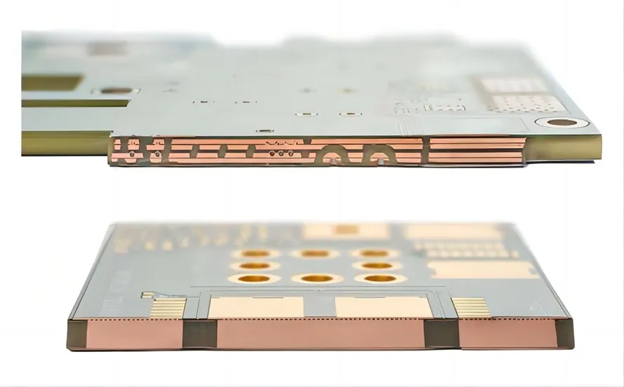
A heavy copper PCB stackup refers to the precise arrangement of conductive copper layers, dielectric cores, and prepregs that form the multilayer structure of a board. In heavy copper designs, outer layers often feature thicker copper foils to support high current densities, while inner layers may vary for signal routing or power distribution. This configuration matters because standard stackups fail under high loads, leading to overheating, voltage drops, or failures in applications requiring robust power delivery. For instance, in power conversion systems, heavy copper PCB stackups enhance thermal management by increasing cross-sectional area for heat spreading. Industry relevance stems from growing demands in electric vehicles and renewable energy systems, where reliability under stress is paramount. Adhering to established guidelines ensures the stackup meets performance criteria without compromising manufacturability.
Core Technical Principles of Heavy Copper PCB Layer Stack
The foundation of heavy copper PCB stackup lies in understanding how copper thickness affects electrical properties. Thicker copper reduces resistance and improves current carrying capacity, but it alters dielectric spacing and field distribution, impacting transmission line characteristics. Engineers calculate layer thicknesses to maintain consistent dielectric heights between planes, as variations can introduce unintended capacitance. Material selection plays a key role; cores and prepregs with matched coefficients of thermal expansion minimize stress during lamination. Sequential lamination processes accommodate heavy copper by building the stackup in stages, preventing defects like voids or delamination. These principles guide the transition from concept to fabrication, ensuring the heavy copper PCB layer stack supports intended functionality.
Heavy copper introduces unique challenges in electromagnetic behavior. Increased skin depth at lower frequencies means more uniform current distribution, beneficial for power traces, yet signal lines require wider geometries to achieve target impedances. Reference planes adjacent to signal layers shield against crosstalk, but heavy copper planes demand careful splitting to avoid impedance discontinuities. Thermal conductivity improves with thickness, aiding heat transfer to the board surface, yet uneven distribution can cause hotspots. Mechanical integrity relies on symmetric construction, where copper weights mirror across the neutral axis to counteract bending moments. By applying these mechanisms, designers optimize the stackup for multifaceted performance.
Optimizing Heavy Copper PCB Impedance Control
Impedance control in heavy copper PCB stackups requires precise adjustments due to the inverse relationship between copper thickness and characteristic impedance. Thicker conductors lower impedance for a given geometry, so engineers widen traces or increase dielectric thickness to compensate while preserving signal quality. Field solvers model the stackup to predict differential or single-ended impedances, accounting for copper roughness and dielectric constants. Prepreg selection influences this; low-loss materials maintain consistency across frequencies. Tolerance stacking in multilayer builds necessitates tight control over core and prepreg thicknesses during pressing. As outlined in IPC-2221 generic design standards, conductor sizing integrates with impedance targets for cohesive layouts.
Maintaining tolerances demands collaboration between design and fabrication teams. Heavy copper etching profiles differ from standard, with trapezoidal shapes affecting effective width, thus simulations incorporate etch factors. Plane capacitance provides return paths, stabilizing impedance, but vias transitioning layers introduce stubs that must be minimized through back-drilling or blind vias. Frequency-dependent effects like dielectric absorption become pronounced in high-speed sections, requiring hybrid stackups with thinner signal layers amid heavy power planes. Verification through test coupons embedded in panels confirms modeled values post-fabrication. These steps ensure heavy copper PCB impedance control aligns with system requirements.
Enhancing Heavy Copper PCB Signal Integrity
Signal integrity in heavy copper PCB stackups hinges on mitigating losses, reflections, and noise in mixed-signal environments. Heavy power layers can couple noise into sensitive traces if ground return paths are inadequate, so dedicated reference planes isolate domains. Length matching and serpentine routing preserve timing for differential pairs routed near heavy copper. Via optimization reduces stub effects; filled or plated-through holes with controlled plating thickness maintain continuity. Crosstalk diminishes with increased spacing, as fields from adjacent heavy traces extend further. Engineers employ guard traces or stitching vias to contain emissions from power sections.
Loss mechanisms intensify with frequency; skin effect confines currents to surfaces, elevating effective resistance in heavy copper. Dielectric losses from prepregs add attenuation, favoring low-Dk materials in signal stacks. Power integrity complements signal efforts by ensuring stable voltages, with heavy copper planes acting as low-inductance reservoirs. Simulations predict eye diagrams, incorporating stackup parasitics for pre-layout validation. Post-route extraction refines models, identifying fixes like additional decoupling. IPC-6012 qualification specifications verify these aspects through electrical testing, confirming heavy copper PCB signal integrity under operational stresses.
Best Practices for Heavy Copper PCB Stackup Design
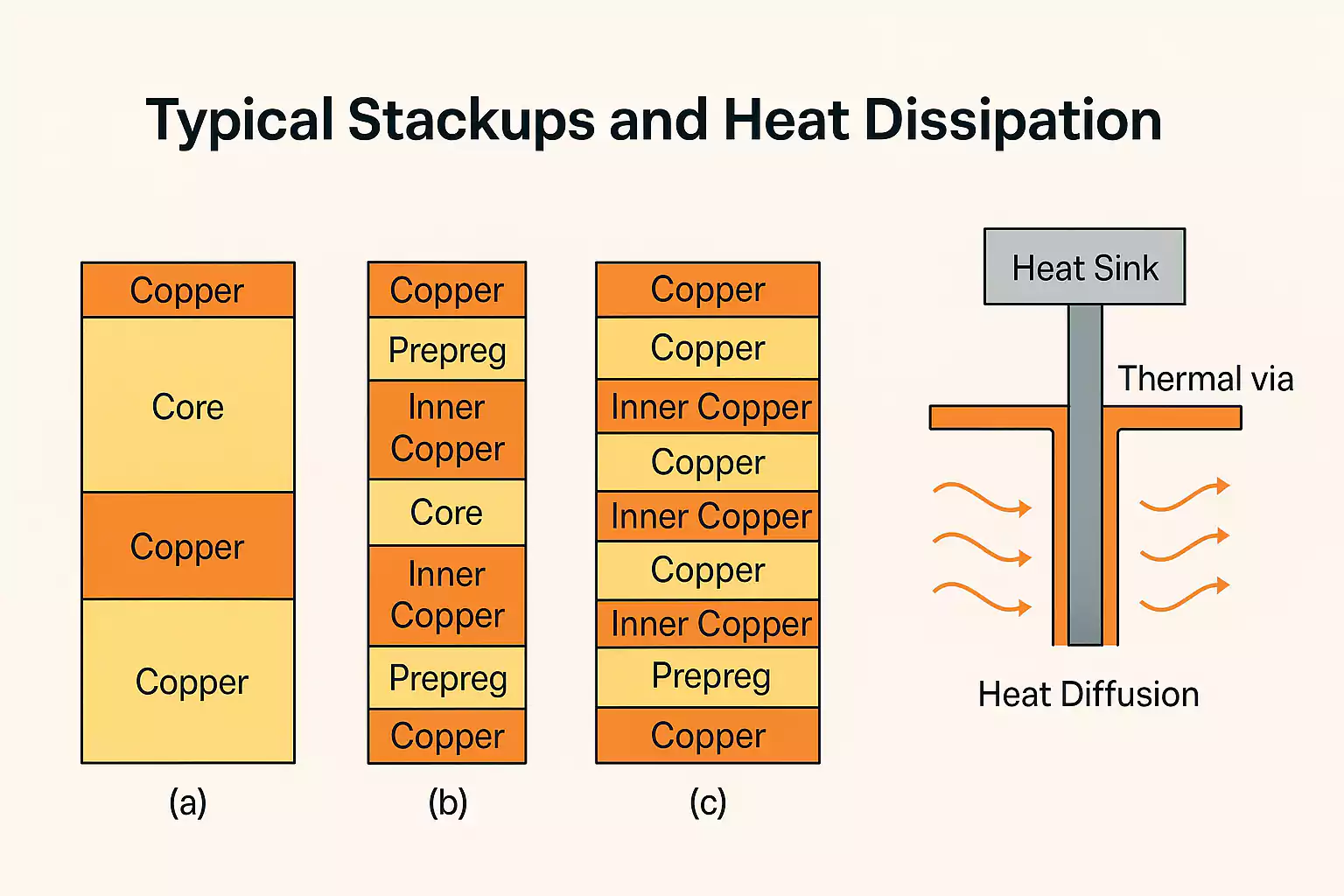
Start with symmetric stackups to balance copper distribution, placing heavy layers on both outer surfaces and mirroring inner configurations. This prevents warpage from CTE mismatches during thermal cycling. Use high-Tg FR-4 or polyimide cores for stability, with prepreg schedules calculated for target dielectric thicknesses. Incorporate thermal vias arrays under hotspots, staggered to maximize density without bridging. Plane design avoids splits under signals; instead, use moats with jumpers for isolation. IPC-2152 standards guide trace widths for current capacity, integrating thermal rise limits into sizing.
Via strategies evolve for heavy copper; aspect ratios below 6:1 ensure plating uniformity, with tenting or plugging for reliability. Sequential build processes layer heavy sections separately, controlling press cycles to avoid resin starvation. Copper balance extends to etch densities, using filler patterns on low-density areas to equalize stress. Fabrication feedback loops refine designs, incorporating panel-level warpage data. Documentation specifies foil weights, etch factors, and impedance targets clearly. These practices yield robust heavy copper PCB stackups optimized for performance.
Addressing Common Challenges in Heavy Copper Designs
Warpage emerges as a primary issue due to asymmetric expansion between thick copper and thinner dielectrics. Mitigation involves neutral axis alignment and controlled cooling post-lamination. Plating buildup in vias risks cracking under thermal stress, addressed by pulse plating for even deposition. Etch undercutting in heavy foils demands compensated artwork with larger clearances. Testing protocols measure bow and twist, rejecting boards exceeding limits. Troubleshooting integrates DFM reviews early, simulating lamination flows.
Reliability testing simulates field conditions, including power cycling and humidity exposure. Filled vias enhance thermal cycling endurance, preventing fatigue. Material qualification ensures compatibility, avoiding voids from mismatched flows. These solutions fortify heavy copper PCB layer stacks against real-world demands.
Conclusion
Effective heavy copper PCB stackup design integrates electrical precision with thermal and mechanical robustness. By prioritizing symmetry, impedance adjustments, and material synergy, engineers achieve superior heavy copper PCB impedance control and signal integrity. Best practices grounded in industry standards deliver reliable performance in high-power scenarios. Future designs will leverage advanced materials and modeling for even greater efficiency. Mastering these elements positions teams to innovate confidently.
FAQs
Q1: What is a heavy copper PCB stackup, and why is it essential for power applications?
A1: A heavy copper PCB stackup arranges thick copper layers with cores and prepregs to handle high currents and heat. It excels in power supplies and inverters by reducing resistance and improving dissipation. Symmetric builds prevent warpage, while layer sequencing supports mixed signals. Essential for reliability under load, it follows design guidelines for optimal heavy copper PCB layer stack performance.
Q2: How does heavy copper affect PCB impedance control?
A2: Thicker copper lowers impedance, requiring wider traces or thicker dielectrics for compensation. Modeling predicts values considering etch profiles and roughness. Reference planes stabilize fields, with tolerances verified via coupons. Critical for high-speed signals amid power layers, it ensures consistent heavy copper PCB impedance control across frequencies.
Q3: What strategies improve signal integrity in heavy copper PCB stackups?
A3: Isolate signals with ground planes, use back-drilled vias to minimize stubs, and match lengths for timing. Low-loss dielectrics reduce attenuation, while stitching contains noise. Simulations validate eye patterns pre- and post-route. These maintain heavy copper PCB signal integrity in demanding mixed environments.
Q4: How to prevent warpage in heavy copper PCB layer stacks?
A4: Employ symmetric copper distribution mirroring weights across the neutral axis. Select matched CTE materials and control lamination pressures. Balance etch densities with fillers and test panels for bow. Sequential processes aid complex builds, ensuring flatness for assembly.


