 ALLPCB


Introduction
Specifying copper thickness in PCB design software is a critical step that bridges conceptual designs with manufacturable boards. Engineers often start with units like mils, where 1 mil equals 0.001 inches, but translating these into real-world foil weights ensures reliable performance. This PCB design software tutorial guides you through the process, covering units, standards, and software-specific settings. Whether handling power traces or high-frequency signals, correct copper thickness prevents overheating, supports current capacity, and maintains impedance control. By following these steps, you align your design with fabrication capabilities from the outset.
Copper thickness directly influences electrical, thermal, and mechanical properties of the PCB. Incorrect settings can lead to trace failures or excessive costs during production. This guide provides logical steps for popular tools, helping electric engineers optimize their workflows efficiently.
What Is Copper Thickness and Why It Matters in PCB Design
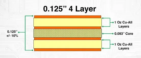
Copper thickness refers to the vertical dimension of the conductive foil laminated onto the PCB substrate, typically measured in ounces per square foot (oz/ft2) or mils. One ounce per square foot corresponds to approximately 1.37 mils or 35 microns nominally, though finished thickness varies after etching and plating. Standard values include 0.5 oz, 1 oz, and 2 oz, selected based on application needs. Thicker copper enhances current-carrying capacity and heat dissipation but increases fabrication complexity and cost.
In high-power designs, adequate thickness prevents excessive temperature rise in traces, as outlined in IPC-2221 guidelines for conductor sizing. For signal integrity in multilayer boards, uniform thickness across layers maintains controlled impedance and reduces crosstalk. Mechanical reliability also benefits, as thicker copper resists warpage under thermal stress. Ignoring these factors risks field failures, making precise specification essential in every PCB design software tutorial.
Fabricators measure finished copper after processing, with IPC-6012 specifying minimum acceptable values for external and internal layers. Engineers must account for plating additions, typically 0.5 to 1 mil on outer layers. This ensures the design matches production outcomes, avoiding iterations.
Technical Principles of Copper Thickness Specification
Copper foil weight determines the base thickness before processing, with conversions like 1 oz equaling 1.37 mils providing a starting point for calculations. During lamination and etching, material is removed, reducing thickness by 10-20% on average. Plating then rebuilds outer layers to meet design targets. Understanding these steps allows engineers to predict final dimensions accurately.
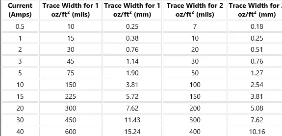
Current-carrying capacity scales with cross-sectional area, where thicker copper supports higher amperage without violating temperature rise limits. IPC-2221 charts relate trace width, thickness, and allowable delta-T, guiding selections for power distribution. For example, doubling thickness from 1 oz to 2 oz can significantly boost ampacity for the same width. Thermal management in dense layouts further justifies heavier copper on power planes.
Impedance control in high-speed designs requires consistent thickness across coupled traces. Variations lead to mismatches, degrading signal quality. Multilayer stackups demand balanced inner and outer layer specs to minimize via resistance and interlayer alignment issues. Standards like IPC-6012 ensure these parameters align with quality classes for rigid boards.
Mechanical aspects include etch factor, where deeper etches in thick copper create trapezoidal profiles, affecting surface finish. Balanced copper distribution prevents board bow and twist, critical for assembly yields. Engineers evaluate these in stackup planning to comply with overall board tolerances.
Factors Influencing Copper Thickness Selection
Application requirements dictate thickness choices, starting with maximum current per trace. Power electronics favor 2 oz or heavier for robustness, while consumer devices stick to 1 oz for cost efficiency. Frequency matters too, as skin effect in RF designs limits effective thickness to microns at GHz ranges.
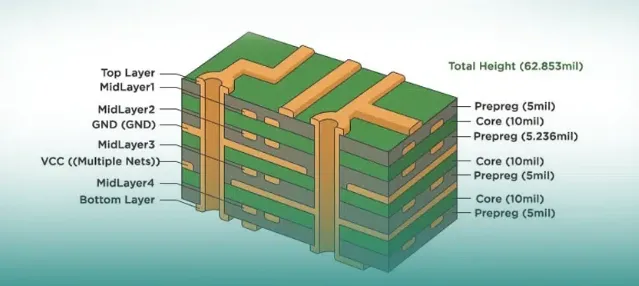
Layer count and stackup configuration influence decisions. Inner layers often use lighter copper, like 0.5 oz, to ease drilling and lamination, while outer layers handle heavier weights. Thermal vias and plane stitching enhance dissipation without sole reliance on thickness.
Cost and lead time rise with heavier copper due to extended plating cycles and handling challenges. DFM rules recommend minimum widths scaling with oz weight, such as 10 mils for 2 oz traces. Early specification in design software prevents downstream revisions.
Environmental factors, including operating temperature and vibration, necessitate margin in thickness for reliability. Compliance with J-STD-001 for soldering processes favors standard weights to ensure consistent wetting.
Practical Solutions: Best Practices for Specifying Copper Thickness
Begin by calculating requirements using IPC-2221-derived tools for trace ampacity, factoring in allowable temperature rise. Select standard weights to match fab capabilities, verifying with stackup simulations. Document specs clearly in fabrication notes for consistency.
Balance copper across layers to avoid warpage, aiming for symmetric buildups in multilayers. Use heavier copper judiciously on power nets, reserving signal layers for standard 1 oz. Validate with thermal analysis software integrated into your design flow.
Incorporate plating allowances, adding 0.7-1 mil to outer layers post-etch. Specify finished thickness targets per IPC-6012 Class 2 or 3 as needed. Prototype testing confirms predictions, adjusting for real-world variances.
Step-by-Step Guide to Copper Thickness Setting in PCB Design Software
Access the layer stackup manager early in the design phase, as changes propagate to routing rules. Set base foil weights per layer, distinguishing inner from outer. Update design rules for minimum trace widths and clearances accordingly.
Setting Copper Thickness in Altium
Open the Layer Stack Manager via Design menu. Select each copper layer and edit the Thickness parameter, entering values like 35 μm for 1 oz. Differentiate Plane layers if using heavier weights. Save and update the board outline. Verify in 3D view for visualization. This Altium copper thickness setup ensures accurate simulations.
Configuring Copper Thickness in Eagle
Navigate to Edit > Design Rules, then the Physical tab. Input copper thickness under Layer Stackup, such as 1.4 mils for standard. Set substrate and solder mask thicknesses for complete profile. Run DRC to flag inconsistencies. Export stackup details for fab drawings. Eagle copper thickness adjustments support precise DFM.
Adjusting Copper Thickness in KiCad
In Pcbnew, go to File > Board Setup > Physical Stackup tab. Double-click layers to set copper thickness, e.g., 35 μm nominal. Configure prepreg and core dielectrics between. Apply changes and inspect in 3D viewer. KiCad copper thickness settings integrate seamlessly with routing.
Re-run impedance calculators post-adjustment to confirm profiles. Generate stackup reports for manufacturers, including oz notations.
Troubleshooting Common Issues with Copper Thickness
Mismatched simulations arise from ignoring etch back, resolved by using finished thickness in models. Excessive warpage signals imbalance, fixed by symmetrizing layers or adding fill zones. High via resistance in heavy copper boards requires larger drills and plating specs.
Impedance deviations post-fab stem from dielectric variations, mitigated by tight thickness tolerances. Overheating traces indicate underspecced ampacity, prompting width increases alongside thickness. Iterative DRC checks catch these early.
Conclusion
Mastering copper thickness specification transforms PCB design software tutorials into production-ready outputs. From mils conversions to software settings, logical steps ensure electrical reliability and manufacturability. Adhering to standards like IPC-2221 and IPC-6012 minimizes risks across power, signal, and thermal domains. Electric engineers benefit from standardized practices that streamline workflows and enhance board performance. Prioritize stackup planning for optimal results in every project.
FAQs
Q1: How do I calculate the right copper thickness for high-current traces in PCB design software?
A1: Use IPC-2221 guidelines to determine trace width and thickness based on current and temperature rise. Input these into your PCB design software tutorial stackup manager for 1 oz or 2 oz selections. Verify with integrated calculators to balance ampacity and heat. This ensures reliable power delivery without redesigns.
Q2: What is the standard copper thickness setting in Altium for a 4-layer board?
A2: In Altium copper thickness configuration, set outer layers to 35 μm (1 oz finished) and inners to 25-30 μm per fab specs. Access Layer Stack Manager to adjust per layer. Update rules for wider traces on power nets. This aligns with common DFM practices.
Q3: Why does Eagle copper thickness affect DRC violations?
A3: Eagle copper thickness settings in Design Rules define minimum widths and clearances scaling with oz weight. Thicker foils require larger traces to prevent shorts. Adjust Physical tab early to pass checks. Proper setup avoids fab rejections.
Q4: Can KiCad handle custom copper thickness for heavy copper PCBs?
A4: Yes, KiCad copper thickness options in Board Setup > Physical Stackup support 70 μm (2 oz) or more. Set per layer for asymmetric builds. Use 3D view to inspect. Ideal for power applications with accurate simulations.
References
IPC-6012E — Qualification and Performance Specification for Rigid Printed Boards. IPC, 2017
IPC-2221B — Generic Standard on Printed Board Design. IPC, 2012
IPC-A-600K — Acceptability of Printed Boards. IPC, 2020
J-STD-001H — Requirements for Soldered Electrical and Electronic Assemblies. IPC, 2018


