 ALLPCB


High-speed digital systems rely on precise control of signal paths to maintain data integrity. Differential impedance plays a central role in this process by defining the characteristic impedance seen by a pair of coupled traces. Engineers use differential pairs to transmit signals in a balanced manner, which helps preserve waveform quality over longer distances and at higher frequencies. Without proper impedance control, reflections and distortions can degrade performance in applications such as data communications and computing interfaces. Effective management of differential impedance therefore forms a foundational requirement in modern printed circuit board design.
What Is Differential Impedance and Why It Matters
Differential impedance represents the opposition to current flow encountered by a signal traveling along two closely coupled conductors that carry equal and opposite currents. This value differs from single-ended impedance because it accounts for the mutual coupling between the traces. Differential pairs consist of these two traces routed in parallel, typically on the same layer or in adjacent layers of the board stackup. In high-speed signaling environments, maintaining consistent differential impedance ensures that the transmitted signal encounters minimal discontinuities.
Impedance matching between the driver, transmission line, and receiver prevents signal reflections that would otherwise distort the received waveform. Common-mode noise, which appears equally on both lines of the pair, is largely rejected when the receiver responds only to the voltage difference between the lines. This inherent noise rejection improves overall system reliability in electrically noisy environments. Industry standards such as those from IPC provide guidelines for verifying that manufactured boards meet the intended impedance targets.
Technical Principles of Differential Impedance
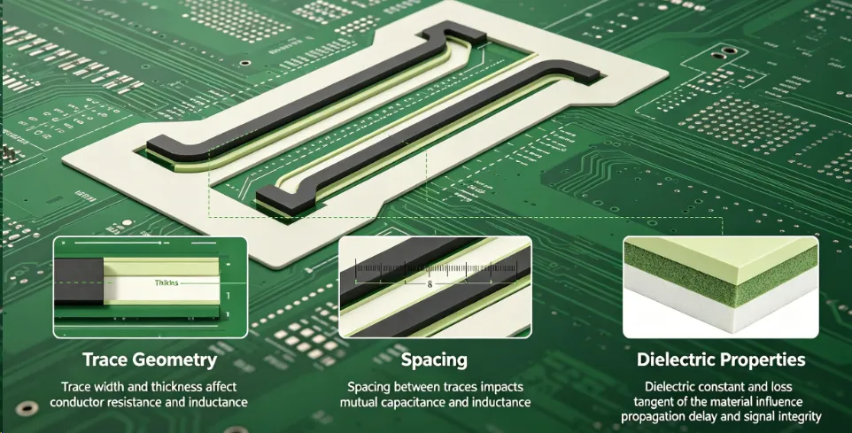
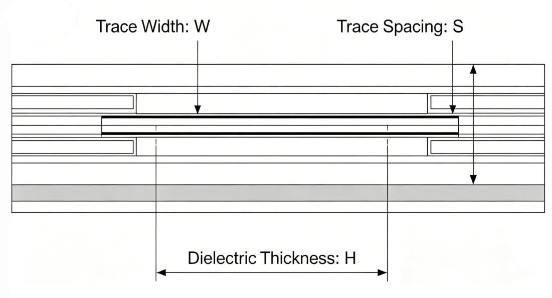
The differential impedance of a pair depends on the geometry of the traces, the spacing between them, the dielectric properties of the surrounding materials, and the reference plane configuration. Trace width and thickness influence the self-inductance and capacitance of each conductor, while the edge-to-edge spacing controls the strength of the mutual coupling. Tighter spacing increases coupling and lowers the resulting differential impedance for a given trace width.
Dielectric constant and thickness of the insulating layers further modulate the capacitance per unit length. When traces are routed on outer layers, the presence of soldermask and air above the copper also affects the final value. Length matching within a pair ensures that both signals arrive simultaneously, preserving the differential relationship throughout propagation. Any deviation in length or geometry introduces skew that can convert differential signals into common-mode components and degrade noise immunity.
Practical Solutions and Best Practices
Designers begin by defining target differential impedance values early in the layout process, typically through stackup planning that selects appropriate dielectric materials and copper weights. Controlled-impedance routing then follows, with trace widths and spacings calculated to achieve the desired value while respecting manufacturing capabilities. Symmetry in the pair routing minimizes unintended coupling to adjacent signals or planes.
Length matching is achieved through serpentine patterns or careful placement rather than abrupt jogs that could create impedance discontinuities. Ground planes or reference layers are positioned consistently beneath differential pairs to provide a stable return path. During fabrication, tolerances on trace width, spacing, and dielectric thickness must remain tight enough to keep the finished impedance within acceptable limits. IPC-6012E outlines qualification requirements that include verification of electrical performance for rigid boards, helping ensure consistency across production lots.
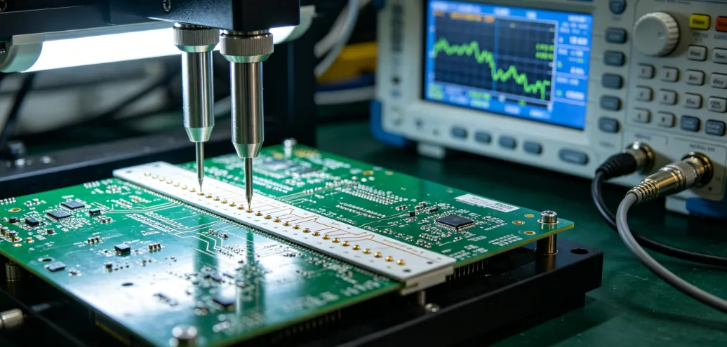
Post-layout simulation using field solvers confirms that the routed geometry meets targets before committing to fabrication. Test coupons fabricated alongside the main board allow measurement of actual impedance on representative structures. IPC-A-600K provides acceptance criteria for the visual and dimensional quality of finished boards, supporting the overall goal of repeatable electrical performance.
Conclusion
Differential impedance control directly supports reliable high-speed signaling by minimizing reflections and rejecting common-mode noise. Structured attention to trace geometry, stackup design, length matching, and manufacturing tolerances enables consistent results across prototypes and production volumes. Adherence to established industry standards further reinforces the repeatability of these outcomes. Engineers who integrate these practices early in the design cycle reduce the likelihood of signal integrity issues that would otherwise require costly revisions.
FAQs
Q1: What is differential impedance in the context of high-speed PCBs?
A1: Differential impedance is the effective impedance presented to a signal traveling along a pair of coupled traces carrying equal and opposite currents. It accounts for both self and mutual inductance and capacitance within the pair. Maintaining a consistent value supports proper impedance matching and reduces reflections during high-speed signaling. Engineers calculate and control this parameter through trace geometry and stackup choices to preserve signal integrity.
Q2: How do differential pairs help reduce common-mode noise?
A2: Differential pairs transmit information as the voltage difference between two lines rather than as an absolute voltage relative to ground. Any noise that couples equally onto both lines appears as common-mode voltage and is rejected at the receiver. This balanced transmission improves immunity in environments where electromagnetic interference is present. Proper impedance control ensures the pair maintains its balanced behavior throughout the signal path.
Q3: Why is impedance matching important for differential signaling?
A3: Impedance matching ensures that the characteristic impedance of the transmission line matches the output impedance of the driver and the input impedance of the receiver. Mismatches cause part of the signal energy to reflect back toward the source, distorting the waveform and increasing bit error rates. In high-speed signaling applications, even small mismatches can limit maximum data rates or operating distances. Controlled differential impedance therefore forms a key element of reliable system design.
Q4: What role do industry standards play in differential impedance control?
A4: Standards establish requirements for board qualification, dimensional tolerances, and acceptance criteria that directly affect the ability to achieve target impedance values. They guide material selection, fabrication processes, and inspection methods used to verify electrical performance. Compliance helps ensure that manufactured boards consistently meet the impedance specifications defined during design.
References
IPC-6012E — Qualification and Performance Specification for Rigid Printed Boards. IPC, 2017
IPC-A-600K — Acceptability of Printed Boards. IPC, 2020





