ALLPCB


Introduction
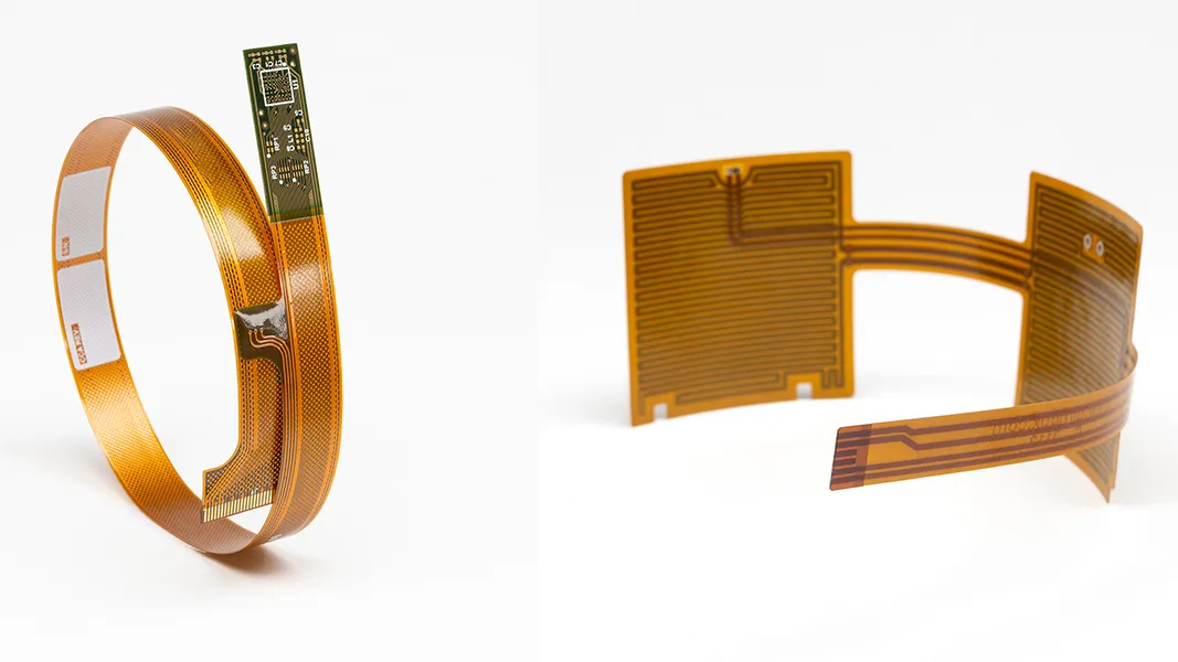
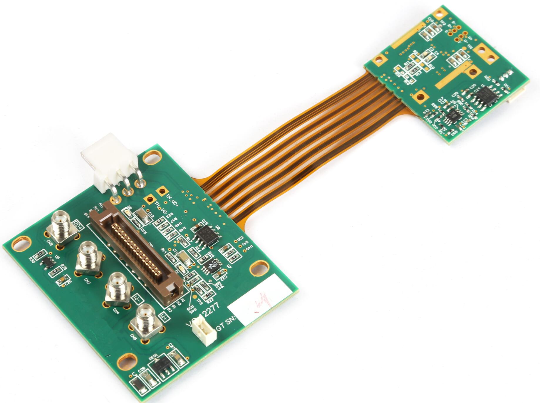
Flexible printed circuit boards, or flex PCBs, have become essential in modern electronics where space constraints and mechanical flexibility are critical. These circuits accommodate dynamic movements in devices like wearables, automotive sensors, and medical implants. Yet, flexible PCB component placement introduces significant challenges due to the inherent bending stress flex PCBs experience during operation. Components mounted in high-strain areas risk failure from fatigue, delamination, or cracked joints, directly impacting flexible circuit reliability. Engineers must balance functionality with mechanical durability to ensure long-term performance. This article delves into these issues from a manufacturing perspective, highlighting principles and solutions grounded in established standards.
Why Component Placement Matters in Flex PCBs
Component placement in flex PCBs determines the overall reliability under mechanical stress. In rigid boards, placement focuses on signal integrity and thermal management, but flex circuits demand consideration of strain distribution during bending. Poor decisions lead to issues like component adhesion flexible circuits weakening, resulting in intermittent failures or complete breakdowns. Factory experience shows that up to a significant portion of flex PCB returns stem from stress-related defects at component sites. Adhering to guidelines ensures strain relief PCB features protect vulnerable areas effectively. Ultimately, strategic placement enhances product lifespan in demanding environments.
The relevance extends to applications involving repeated flexing, where even minor misplacements amplify over cycles. Manufacturers observe that designs ignoring bend zones suffer higher rejection rates during qualification tests. Flexible circuit reliability hinges on anticipating real-world stresses from the outset. Engineers targeting electric engineers appreciate how these factors influence design iterations and production yields. Prioritizing placement aligns with quality control processes in high-volume assembly.
Technical Principles of Bending Stress in Flex PCBs
Bending induces nonuniform stress across the flex PCB cross-section, with the outer layers experiencing tensile forces and inner layers compressive ones. This strain gradient peaks at the neutral axis shift, influenced by material thickness and copper weight. Components placed near bend radii encounter amplified forces, leading to solder joint fatigue or adhesive degradation. Per IPC-2223, bend areas should remain component-free to minimize these risks, as stress concentrations can exceed material yield limits. Understanding strain profiles requires analyzing the minimum bend radius relative to circuit thickness.
Material properties play a key role in stress propagation. Polyimide substrates offer high flexibility but transmit strain to mounted elements like resistors or ICs. Component leads or bodies act as stress risers, promoting cracks under cyclic loading. Factory-driven insights reveal that dynamic applications, such as hinge mechanisms, demand tighter control over placement to avoid delamination at interfaces. Adhesion between components and flex substrate must withstand shear and peel forces during flexure. These mechanisms underscore the need for precise modeling in design phases.
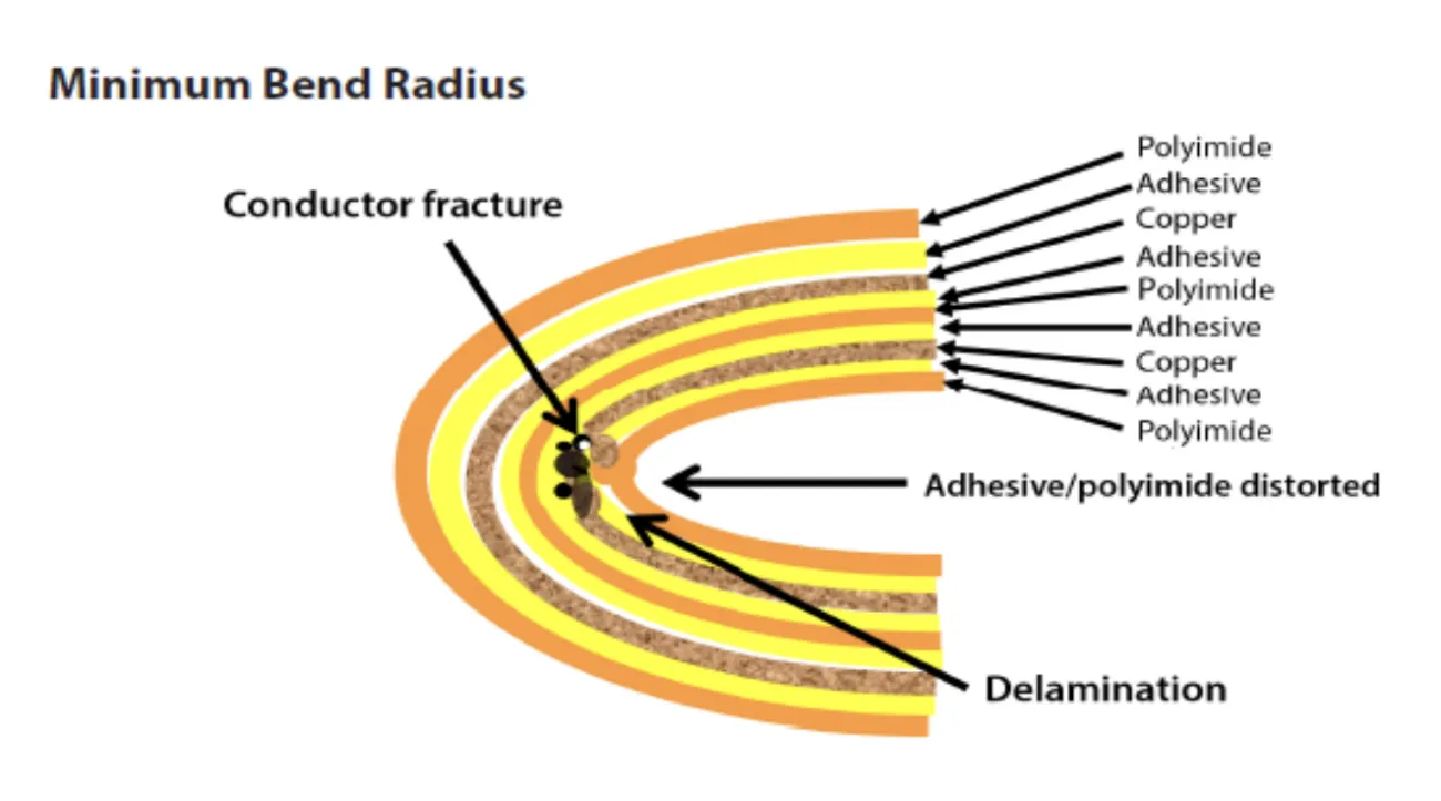
Trace routing intersects with component placement, as conductors in bend zones elongate or contract. Vias and pads near flex regions face similar vulnerabilities, potentially causing open circuits. IPC-6013 outlines performance specs that include flex endurance testing to validate designs against such failures. Engineers must calculate strain relief PCB margins based on expected bend cycles and angles. Ignoring these principles results in field failures, emphasizing proactive stress analysis.
Key Challenges in Flexible PCB Component Placement
One primary challenge is positioning components away from high-stress bend zones while maintaining electrical efficiency. Flex PCBs often feature designated rigid islands for populated areas, but transitions demand careful zoning. Components in semi-flex regions suffer from differential expansion during bending stress flex PCBs impose. This leads to challenges in component adhesion flexible circuits, where epoxies or underfills fail prematurely. Manufacturing tolerances exacerbate issues if alignment drifts during assembly.
Another hurdle involves dynamic versus static bending. Static bends allow looser placement rules, but dynamic scenarios require wider exclusion zones. Strain concentrations at component edges promote microcracks in solder, detectable only after extensive cycling. Flexible circuit reliability suffers when heavy or tall components amplify leverage effects. Factories report higher defect rates in designs crowding bend perimeters. Balancing density with durability remains a core engineering trade-off.
Vibration and thermal cycling compound bending stresses, accelerating fatigue in poorly placed parts. Adhesives must bond under varying humidity and temperatures without embrittling. IPC-2223 provides zoning diagrams to guide placement, preventing overlaps with flex tails. Engineers face decisions on orientation, with parallel-to-bend alignments faring better than perpendicular ones. These challenges highlight the factory perspective on yield optimization through design foresight.
Practical Solutions and Best Practices
Optimal flexible PCB component placement starts with defining bend zones early in layout. Keep active components on rigid sections or straight flex runs, reserving curves for tails only. This strategy, aligned with IPC-2223, reduces bending stress flex PCBs by isolating populated areas. Use teardrop pads and wider traces at transitions for strain relief PCB implementation. Factory processes benefit from these measures, lowering assembly defects and enhancing test passes.
Implement strain relief features like anchor tabs or stitched vias at flex-rigid interfaces. These distribute loads evenly, preventing peel-up during flexure. Select low-modulus adhesives for component adhesion flexible circuits to accommodate movement without cracking. Orient components with leads parallel to the bend axis to minimize shear. Simulation tools verify stress before fabrication, but physical prototypes confirm real-world behavior.
For high-reliability applications, incorporate coverlay cutouts or slotted reliefs near components. Dynamic flex demands repeated bend testing per IPC-6013 to qualify designs. Layer stackups influence outcomes, with thinner copper easing radius compliance. Post-assembly, conformal coatings add protection against environmental factors. These practices boost flexible circuit reliability, as validated in production runs.
Troubleshooting Common Placement Issues
In manufacturing, engineers troubleshoot delamination by inspecting bend radii against specs. If components lift during flex tests, reposition to non-bend areas or reinforce with underfill. Solder joint cracks often trace to perpendicular lead orientations; realign for parallelism. Adhesion failures signal incompatible materials; switch to flexible epoxies tested for peel strength. Cycle testing reveals latent weaknesses early, guiding revisions.
Vibration-induced shifts require damping features like edge stiffeners. Factory data logs correlate placement errors with failure modes, informing DFM feedback. Addressing these iteratively improves yields. Collaboration between design and production teams accelerates fixes.
Conclusion
Navigating component placement challenges in flexible PCBs demands a deep understanding of bending mechanics and stress distribution. Strategic zoning, strain relief PCB techniques, and robust adhesion ensure enduring performance. Standards like IPC-2223 and IPC-6013 provide the framework for reliable designs. Factory insights reinforce that proactive measures yield the highest flexible circuit reliability. Electric engineers can leverage these principles to innovate without compromising durability. Prioritizing these considerations elevates product quality in flex-intensive applications.
FAQs
Q1: What are the main guidelines for flexible PCB component placement near bend areas?
A1: Avoid placing components directly in high-strain bend zones as per IPC-2223 to prevent bending stress flex PCBs from causing failures. Position them on rigid sections or straight flex tails with at least a minimum exclusion distance based on bend radius. Use strain relief PCB features like anchors for transitions. This approach maintains flexible circuit reliability under dynamic conditions. Factory testing confirms these zones reduce defect rates significantly.
Q2: How does bending stress affect component adhesion in flexible circuits?
A2: Bending induces tensile and shear forces that challenge component adhesion flexible circuits, leading to delamination over cycles. Select adhesives with high peel strength and low modulus to absorb strain. Orient components parallel to the bend axis for even distribution. Proper surface preparation enhances bonding. These steps ensure long-term integrity in flexed environments.
Q3: What role does strain relief play in flexible PCB reliability?
A3: Strain relief PCB elements like teardrops and tabs mitigate stress concentrations at component sites during bending. They distribute loads, preventing cracks in solder or substrate. Implement them at all flex interfaces per design standards. This boosts flexible circuit reliability in applications with repeated flexing. Manufacturers prioritize these for qualification success.
Q4: Why is IPC-2223 critical for managing bending stress in flex PCBs?
A4: IPC-2223 outlines bend radius rules and placement restrictions to combat bending stress flex PCBs. It defines safe zones, layer guidelines, and testing protocols. Adhering ensures mechanical endurance. Engineers use it to optimize layouts for reliability. Factory compliance streamlines production and reduces returns.
References
IPC-2223C — Sectional Design Standard for Flexible/Rigid-Flex Printed Boards. IPC, 2019
IPC-6013D — Qualification and Performance Specification for Flexible and Rigid-Flex Printed Boards. IPC, 2014