 ALLPCB


Introduction
Component placement plays a critical role in LED PCB design, particularly for applications demanding high reliability and efficiency. In LED lighting systems, improper positioning of components can lead to excessive heat buildup, reduced luminous output, and premature failure. Engineers must prioritize thermal management LED PCBs to ensure optimal performance under continuous operation. This article explores structured approaches to component placement lighting, drawing on established engineering principles. By following these best practices, designers can enhance LED heat dissipation and extend system lifespan. High brightness LED PCB designs benefit most from meticulous planning in this area.
Why Component Placement Matters in LED Lighting PCBs
LEDs convert electrical energy into light, but a significant portion manifests as heat at the semiconductor junction. This heat must dissipate effectively to maintain junction temperatures below critical thresholds, preserving efficiency and color stability. Poor component placement concentrates heat sources, creating hotspots that degrade performance across the board. In high brightness LED PCB applications, such as street lighting or displays, uneven thermal distribution accelerates solder joint fatigue and material degradation. Component placement lighting directly influences airflow paths and conduction routes, impacting overall system reliability. Adhering to guidelines from IPC-2221C ensures designs meet performance expectations in demanding environments.
Strategic placement minimizes thermal gradients, allowing uniform heat spreading through copper layers and substrates. Clustering LEDs or drivers exacerbates local overheating, while balanced layouts promote natural convection. Electrical considerations, like trace lengths and signal integrity, intersect with thermal needs, requiring holistic optimization. Mechanical stability during assembly and operation also depends on placement, avoiding stress points near board edges. Ultimately, effective component placement lighting supports compliance with quality standards and reduces field failures.

Key Technical Principles Governing Component Placement
Heat transfer in LED PCBs occurs via conduction, convection, and radiation, with conduction dominating within the board. The thermal resistance from LED junction to ambient (Rθja) depends on pad connections, via arrays, and plane areas. Placement influences these paths by determining proximity to heat sinks or chassis. For high brightness LED PCB designs, engineers calculate thermal paths early, considering material conductivity like that of metal-core substrates. Vias under thermal pads bridge layers, channeling heat downward or to ground planes.
Component orientation affects convection; vertical profiles enhance airflow compared to flat layouts. Spacing between components prevents shadowing, ensuring even cooling across the array. Electrical isolation must balance with thermal connectivity, using spokes or relief patterns as per IPC-2221C for pad connections. Board warpage from asymmetric placement alters contact with heatsinks, compromising dissipation. Simulations validate these principles, revealing gradients before prototyping.
Best Practices for Thermal Management in LED PCB Design
Distribute high-power LEDs evenly across the board to avoid localized hotspots. Position them symmetrically relative to mounting holes and airflow inlets for uniform cooling. In linear arrays for lighting strips, maintain consistent inter-LED spacing to equalize current sharing and heat load. Avoid placing sensitive components like capacitors directly adjacent to LEDs; instead, route them to cooler zones. This approach aligns with thermal management LED PCBs principles, promoting longevity.
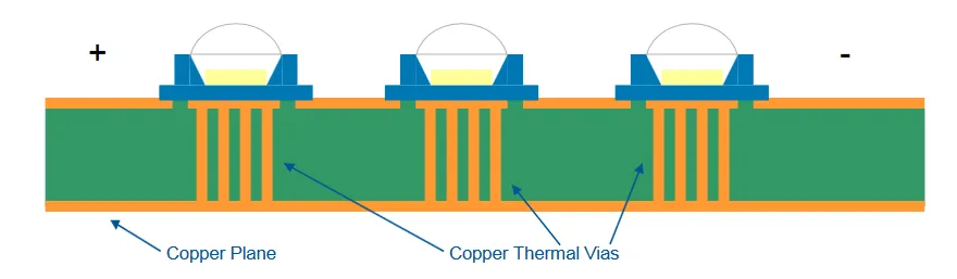
Incorporate thermal vias in arrays beneath LED pads to transfer heat to inner layers or the opposite side. Use plated or filled vias to prevent solder wicking during assembly, ensuring reliable paths. Connect these to large copper pours acting as heat spreaders, extending from component to board edges. For multi-layer boards, dedicate inner layers to ground planes with minimal interruptions. These strategies enhance LED heat dissipation without increasing board size.
Orient components to maximize surface area exposure to airflow. Tall profiles on power devices facilitate chimney effects in enclosed fixtures. Place drivers and resistors downstream of LEDs in expected airflow to utilize pre-heated air without critical overheating. Maintain adequate clearances around vias and pads per assembly tolerances, facilitating inspection and rework. Simulate airflow with board geometry to refine orientations.
Optimizing Component Placement for Electrical and Mechanical Reliability
Beyond thermal aspects, placement ensures short, wide traces for low voltage drop in high-current LED arrays. Group power and ground returns closely to minimize inductance, supporting fast switching if dimming circuits are involved. Signal traces for control should route away from high-current paths to reduce noise coupling. Mechanical fiducials and edge clearances prevent damage during handling and panelization.
For high brightness LED PCB assemblies, follow J-STD-001J guidelines for component positioning to achieve consistent solder joints. Balance mass distribution to mitigate reflow warpage, especially on thick copper or metal-core boards. Secure mounting points near heavy components to withstand vibration in lighting installations. Iterative design reviews incorporate feedback from thermal modeling and DFM analysis.
Advanced Strategies for High Brightness LED PCB Heat Dissipation
Employ metal-core PCBs (MCPCBs) for superior in-plane conductivity in dense arrays. Position LEDs directly over the core interface for shortest conduction paths. Hybrid stacks with FR-4 signal layers over aluminum cores balance cost and performance. External heatsinks attach via screws or clips at optimized locations, informed by placement.
Active cooling, like fans, requires directing airflow over hottest zones defined by placement. Passive fins integrate with board edges for compact designs. Monitor junction temperatures with embedded sensors placed near critical LEDs. These tactics, combined with IEC 62326-20 for high-brightness LED boards, ensure robust thermal management LED PCBs.
Conclusion
Effective component placement lighting forms the foundation of successful LED PCB design. By distributing heat sources evenly, leveraging thermal vias, and optimizing orientations, engineers achieve superior LED heat dissipation. Adhering to standards like IPC-2221C and J-STD-001J guarantees manufacturability and reliability. High brightness LED PCB projects demand these practices to meet efficiency targets and lifespan goals. Implementing simulations early refines layouts, minimizing iterations. Ultimately, thoughtful placement elevates thermal management LED PCBs from good to exceptional.
FAQs
Q1: What are the main factors in LED PCB design for thermal management LED PCBs?
A1: Thermal management LED PCBs hinges on even component distribution, thermal vias under pads, and copper planes for spreading. Placement near airflow paths enhances convection, while materials like MCPCBs conduct heat efficiently. Simulations predict hotspots, guiding refinements. Following IPC-2221C ensures balanced electrical and thermal performance without hotspots.
Q2: How does component placement lighting impact high brightness LED PCB reliability?
A2: Component placement lighting prevents hotspots by spacing LEDs uniformly and isolating sensitive parts. This reduces junction temperatures, preserving lumen maintenance over time. Vias and planes channel heat away, aligning with IEC 62326-20 for high-brightness applications. Poor clustering accelerates degradation, while optimized layouts extend operational life significantly.
Q3: What role do thermal vias play in LED heat dissipation?
A3: Thermal vias in LED heat dissipation transfer heat from top-side pads to lower layers or cores. Arrays under LEDs provide low-resistance paths, preventing solder issues per assembly standards. Plating enhances conductivity, integrating seamlessly with ground planes. Proper sizing and spacing maintain electrical isolation while maximizing thermal relief.
Q4: Why avoid clustering components in high brightness LED PCB designs?
A4: Clustering in high brightness LED PCB designs creates thermal gradients, risking failures from overheating. Even distribution promotes uniform cooling via conduction and convection. This practice supports compliance with J-STD-001J for reliable soldering. Balanced layouts also minimize warpage, ensuring stable heatsink contact.
References
IPC-2221C — Generic Standard on Printed Board Design. IPC, 2023
J-STD-001J — Requirements for Soldered Electrical and Electronic Assemblies. IPC, 2024
IEC 62326-20 — Printed boards – Part 20: Printed circuit boards for high-brightness LEDs. IEC, 2016


