 ALLPCB


Introduction
Blind vias play a critical role in modern automotive PCBs, enabling higher routing density in compact designs required for advanced driver-assistance systems and power electronics. These vias connect surface layers to inner layers without penetrating the entire board, optimizing space while maintaining signal integrity under harsh operating conditions. In automotive applications, where PCBs face extreme temperatures, vibrations, and humidity, blind vias must meet stringent reliability standards to prevent failures that could compromise vehicle safety. Electrical engineers designing these boards need to balance performance demands with manufacturability constraints. This article explores blind via automotive applications, automotive PCB design guidelines, blind via reliability testing automotive protocols, and automotive electronics PCB manufacturing processes. Understanding these elements ensures PCBs deliver consistent performance over the vehicle's lifecycle.
The relevance of blind vias in automotive PCBs stems from the industry's push for electrification and autonomy. Power distribution modules and sensor interfaces demand multilayer stacks where blind vias minimize inductance and improve thermal dissipation. Engineers must consider how these vias interact with surrounding copper traces and dielectrics during operation. Poor design can exacerbate issues like electromigration under high currents typical in battery management systems. By integrating blind vias thoughtfully, designers achieve compliance with performance benchmarks while enhancing overall board robustness. This approach supports the evolution toward more integrated and efficient automotive electronics.
What Are Blind Vias and Why Do They Matter in Automotive PCBs?
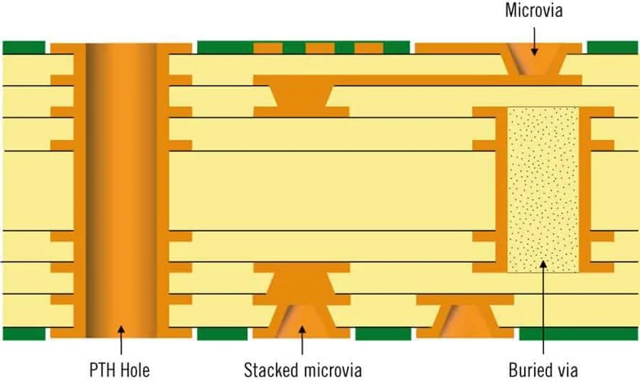
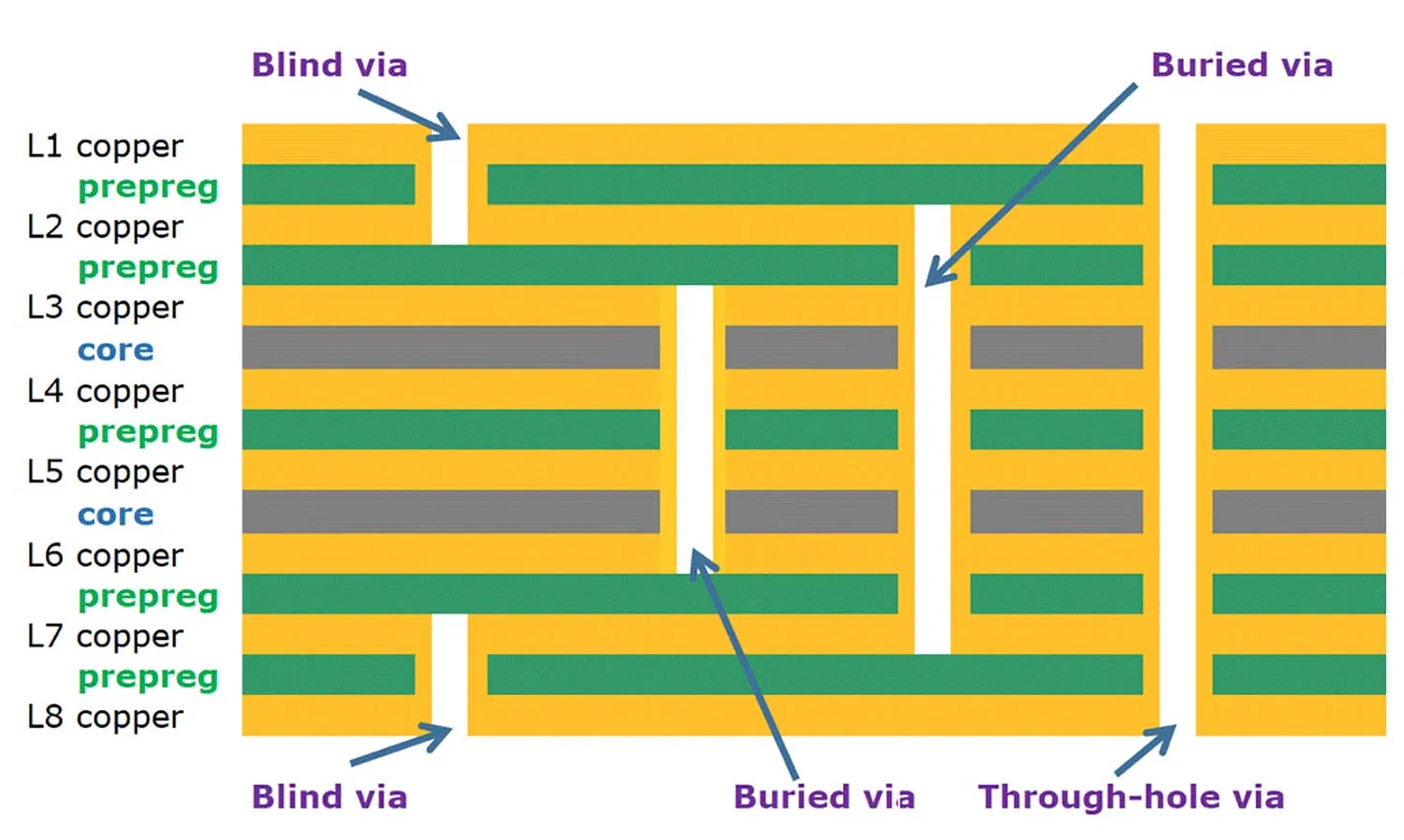
Blind vias are plated holes that start from an outer layer and terminate at an inner layer, unlike through-hole vias that span the full board thickness. This design frees up inner layer real estate for routing, which is essential in high-density interconnect boards used in engine control units and infotainment systems. In automotive environments, space constraints and signal speed requirements drive the adoption of blind vias to support faster data transmission and reduced electromagnetic interference. Their implementation allows for more layers without increasing board size, aligning with the miniaturization trends in electric vehicles. However, the partial depth introduces unique challenges in plating uniformity and thermal stress management. Reliability becomes paramount, as failures like via cracking can lead to intermittent connections in safety-critical systems.
The relevance of blind vias in automotive PCBs stems from the industry's push for electrification and autonomy. Power distribution modules and sensor interfaces demand multilayer stacks where blind vias minimize inductance and improve thermal dissipation. Engineers must consider how these vias interact with surrounding copper traces and dielectrics during operation. Poor design can exacerbate issues like electromigration under high currents typical in battery management systems. By integrating blind vias thoughtfully, designers achieve compliance with performance benchmarks while enhancing overall board robustness. This approach supports the evolution toward more integrated and efficient automotive electronics.
Technical Principles of Blind Vias in PCB Design and Manufacturing
The fabrication of blind vias begins with sequential lamination, where cores are built incrementally to expose specific layers for drilling. Mechanical or laser drilling creates the via cavity, followed by electroless copper deposition and electroplating to form a conductive barrel. Aspect ratios typically stay below 1:1 for laser-drilled vias to ensure plating coverage, preventing voids that compromise conductivity. In automotive electronics PCB manufacturing, material selection influences via integrity, with low-loss dielectrics resisting delamination under thermal loads. The plating thickness must provide a robust barrier against corrosion in humid engine compartments. Engineers evaluate stack-up configurations to position blind vias away from high-stress zones.
Signal propagation through blind vias requires controlled impedance matching, achieved by adjusting pad sizes and anti-pad clearances per established design rules. The stub absence in blind vias reduces reflections compared to through vias, benefiting high-speed signals in radar modules. However, the fill material, often conductive epoxy, must withstand shear forces from coefficient of thermal expansion mismatches. Manufacturing processes incorporate plasma cleaning to enhance adhesion before plating. Cross-section analysis verifies via geometry post-fabrication, identifying issues like dog-boning or barrel cracks early. These principles underpin reliable performance in demanding automotive scenarios.
Automotive PCB Design Guidelines for Blind Vias
Automotive PCB design guidelines emphasize via placement to avoid board edges and flex zones, minimizing mechanical fatigue. Blind vias should cluster in low-vibration areas, with staggered positioning across layers to distribute stress evenly. Pad diameters exceed drill size by at least 300 microns post-plating, ensuring annular ring integrity for current carrying. Layer sequencing optimizes blind via spans, limiting them to adjacent layers where possible to simplify fabrication. Signal nets use dedicated via farms for redundancy in critical paths. These practices align with IPC-2221 guidelines for general PCB design, adapted for automotive rigor.
Thermal management integrates blind vias into heat dissipation paths, often filled with thermal conductive paste under power components. Clearance rules prevent shorting during reflow soldering, with solder mask registration critical over via openings. For high-frequency applications, engineers model via transitions using field solvers to predict discontinuities. Automotive standards demand Class 3/A qualification, influencing via density limits. Documentation includes stack-up drawings specifying blind via locations and depths. Adhering to these guidelines streamlines automotive electronics PCB manufacturing and reduces iteration cycles.
Blind Via Reliability Testing in Automotive Applications
Blind via reliability testing automotive protocols simulate real-world stressors to validate long-term performance. Thermal cycling exposes boards to repeated temperature swings, assessing via barrel cracking from expansion differentials. Highly accelerated stress tests combine temperature, humidity, and bias to accelerate corrosion and electromigration. Vibration testing per automotive profiles evaluates solder joint and via anchorage under harmonic loads. Electrical continuity monitoring detects opens during these sequences. IPC-6012DA outlines qualification for boards in high-vibration environments, guiding test severity.
Post-test analysis involves dye-and-peel for microcrack detection and scanning electron microscopy for plating integrity. Failure modes like via piston-ing or resin smear highlight design flaws. Accelerated life testing extrapolates field reliability using Arrhenius models, though conservative margins apply for safety systems. Automotive PCB design guidelines incorporate margining based on these results. Iterative testing refines via fill methods and material choices. Comprehensive protocols ensure blind vias withstand 10-15 years of service life.
Best Practices for Implementing Blind Vias in Automotive Designs
Start with simulation-driven design, modeling thermomechanical stresses to predict via fatigue. Select laminates with matched CTE to copper for blind via stacks, reducing interfacial shear. Employ filled vias in power planes to block solder wicking and enhance thermal conductivity. Manufacturing partners should confirm sequential build capabilities for complex blind via arrays. Design for testability includes daisy-chain nets for in-circuit verification. These steps embody automotive PCB design guidelines for robust outcomes.
Fabrication control involves X-ray inspection for via fill density and capacitance testing for plating voids. Post-laminate etching ensures clean via walls before plating. For high-reliability, consider staggered blind vias over stacked to improve yield. Documentation specifies tolerance stacks for depth control. Field feedback loops refine future designs. Practical adherence elevates blind via automotive applications to production readiness.
Conclusion
Blind vias enable compact, high-performance automotive PCBs by optimizing routing density and signal quality. Automotive PCB design guidelines and rigorous reliability testing ensure these features withstand operational extremes. From sequential fabrication to stress qualification, each step builds toward dependable electronics. Electrical engineers benefit from structured approaches that integrate standards like IPC-6012DA and IPC-2221. Prioritizing these elements delivers boards meeting automotive demands. Future advancements will further refine blind via technologies for next-generation vehicles.
FAQs
Q1: What are key automotive PCB design guidelines for blind vias?
A1: Blind via automotive applications require staggered positioning, aspect ratios under 1:1, and pad oversizing by 300 microns minimum. Stack-ups limit spans to adjacent layers for plating reliability. Simulate thermomechanical stresses and select CTE-matched materials. These practices per IPC-2221 enhance manufacturability and performance in high-density boards.
Q2: How is blind via reliability testing conducted for automotive PCBs?
A2: Blind via reliability testing automotive involves thermal cycling, HAST, and vibration per qualification protocols. Dye-and-peel detects microcracks, while electrical monitoring tracks continuity. IPC-6012DA guides high-vibration assessments. Results inform design margins for 10+ year lifecycles in engine compartments.
Q3: Why use blind vias in automotive electronics PCB manufacturing?
A3: Blind vias save inner layer space in multilayer stacks for ECUs and sensors, reducing inductance for high-speed signals. They support dense routing without full-board penetration. Automotive electronics PCB manufacturing uses sequential lamination for precision. Reliability testing validates endurance under thermal and mechanical loads.
Q4: What challenges arise with blind vias in automotive applications?
A4: Challenges include plating voids, thermal fatigue cracking, and aspect ratio limits in blind via automotive applications. Vibration induces piston-ing, addressed by fills and anchoring. Automotive PCB design guidelines mitigate via design guidelines via simulation and testing. Proper stack-up planning overcomes these for robust performance.
References
IPC-6012DA — Qualification and Performance Specification for Rigid Printed Boards in Automotive Applications. IPC, 2015
IPC-2221B — Generic Standard on Printed Board Design. IPC, 2012
IPC-9701 — Performance Test Methods and Qualification Requirements for Surface Mount Solder Attachments. IPC, 2019


