 ALLPCB


Automated functional testing has become a cornerstone of modern electronics manufacturing. It verifies that assembled printed circuit boards perform their intended functions under realistic operating conditions. In high-volume production environments, this approach replaces manual probing with repeatable, software-driven sequences that run on automated test equipment. Engineers rely on these systems to catch defects that visual inspection or basic continuity checks might miss. The result is faster throughput without sacrificing the reliability required for complex assemblies.
Automated functional testing applies a series of electrical stimuli to a finished PCB and measures its responses against predefined specifications. Unlike in-circuit testing that checks individual components, functional testing evaluates the board as a complete system. This distinction matters because many defects only appear when the circuit operates as designed. In high-volume testing, the process runs continuously on production lines, feeding data directly into quality-management databases. Manufacturers therefore gain immediate visibility into process drift or recurring faults.
What Automated Functional Testing Means for PCB Validation
Industry standards such as IPC-6012E guide the qualification criteria that automated functional testing must satisfy. These criteria define acceptable performance limits for parameters such as voltage levels, timing margins, and signal integrity. When a board passes the automated sequence, it receives a traceable record that supports downstream traceability requirements. The method therefore integrates naturally with broader quality systems without introducing new documentation overhead.
Technical Principles Behind Automated Test Equipment
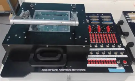
Automated test equipment executes test programs written in hardware-description or scripting languages. The equipment applies power, clocks, and digital or analog signals through a bed-of-nails fixture or edge-connector interface. Sensors inside the equipment capture voltage, current, frequency, and logic states at multiple test points. Software then compares these measurements against expected values stored in a test database. Any deviation triggers an automatic fail flag and logs the exact test step for root-cause analysis.
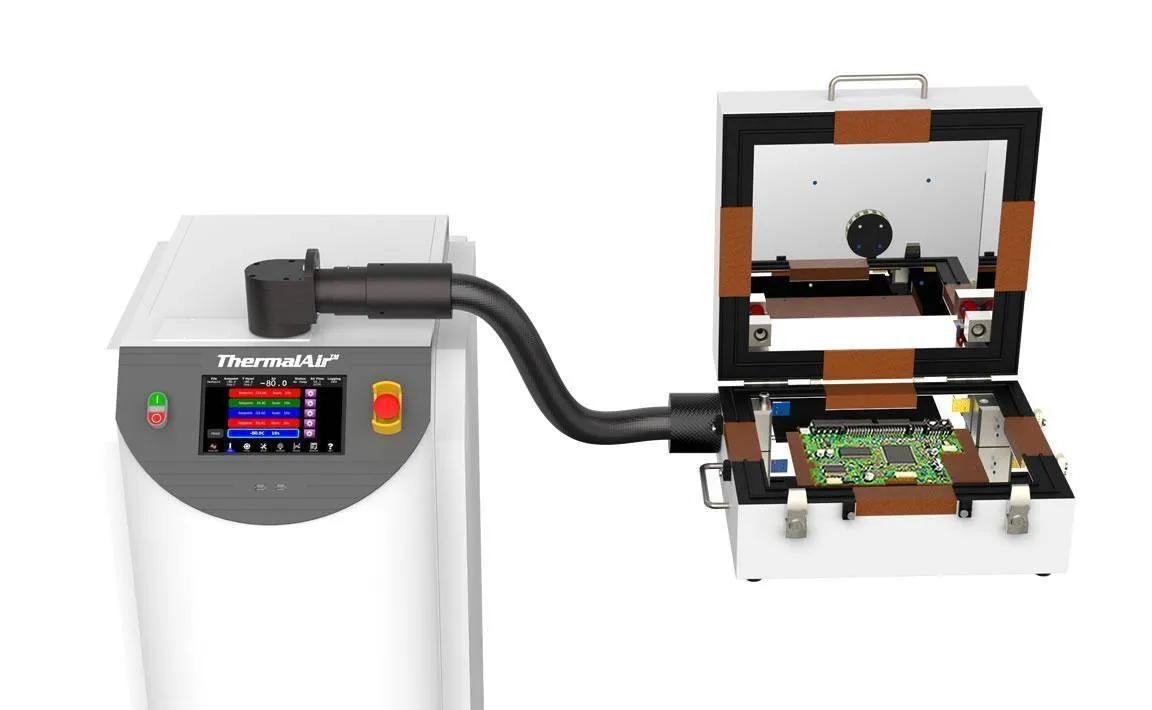
Signal integrity remains a primary concern during high-speed functional tests. Parasitic inductance and capacitance in the fixture can distort waveforms, so fixture design follows strict layout rules derived from IEC standards. Temperature control is another critical factor; many functional tests include thermal cycling to simulate real-world conditions. The combination of electrical and environmental stress reveals marginal components that would otherwise pass at room temperature.
Practical Solutions and Best Practices in High-Volume Environments
Successful deployment begins with clear test coverage goals defined during the design-for-test phase. Engineers review schematic and layout files to identify nodes that must be accessible through the fixture. They then prioritize tests that exercise critical paths such as power sequencing, communication buses, and sensor interfaces. This prioritization keeps cycle time within production takt requirements while still achieving high fault coverage.
Fixture maintenance schedules prevent intermittent contact issues that can masquerade as board failures. Regular cleaning and pin replacement, performed according to documented intervals, maintain consistent measurement accuracy. Data from the automated test equipment also feeds statistical process control charts. Trend analysis of pass/fail rates highlights when process adjustments are needed before defects reach the customer.
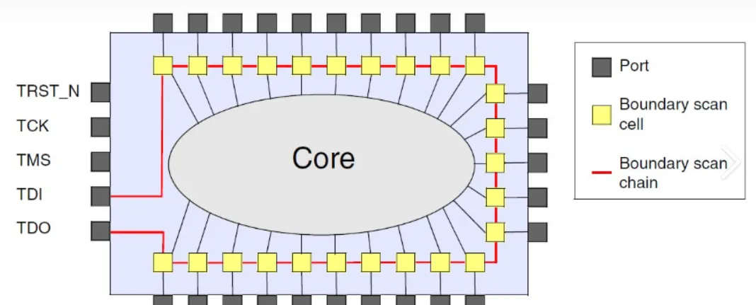
Another effective practice is the use of boundary-scan techniques where applicable. These techniques allow the test system to control and observe internal nodes without physical probing. When combined with functional vectors, boundary scan increases coverage for complex digital devices while reducing the number of physical test points required.
Troubleshooting Common Issues in Automated Functional Testing
When a test station reports an unexpectedly high failure rate, engineers first verify fixture alignment and contact resistance. A simple four-wire measurement on a known-good board quickly isolates mechanical problems from genuine board defects. Next, they examine the test program for timing violations or incorrect tolerance settings. Adjusting these parameters often restores yield without altering the product design.
Thermal-related failures require separate investigation. Boards that pass at ambient temperature may fail after a short soak period. In such cases, engineers review the thermal profile used during testing and compare it against the expected operating range defined in the product specification. This comparison usually reveals whether the test condition is overly stringent or whether a component is operating near its limit.
Conclusion
Automated functional testing provides a repeatable, data-rich method for validating PCBs in high-volume production. By focusing on system-level behavior rather than isolated components, it catches defects that would otherwise escape earlier inspection stages. When implemented with attention to fixture design, test coverage, and statistical feedback, the approach supports both quality targets and production throughput. Engineers who integrate these practices early in the product lifecycle obtain measurable improvements in first-pass yield and reduced warranty returns.
FAQs
Q1: What distinguishes automated functional testing from in-circuit testing for PCB validation?
A1: Automated functional testing applies power and signals to the fully assembled board and verifies that the complete circuit performs its intended functions. In-circuit testing checks individual components for correct placement and basic continuity. The two methods complement each other, but functional testing is essential for confirming system-level behavior in high-volume testing environments.
Q2: How does automated test equipment improve throughput in high-volume PCB production?
A2: Automated test equipment executes pre-programmed sequences in seconds per board, eliminating manual probing and subjective judgment. Results are logged automatically, enabling immediate statistical analysis and process adjustments. This speed and consistency allow production lines to maintain takt time while still meeting the quality requirements outlined in IPC-6012E.
Q3: What role do industry standards play in defining automated functional test limits?
A3: Standards such as JEDEC J-STD-020E establish environmental stress conditions and acceptance criteria that automated functional testing must incorporate. These criteria ensure that test conditions reflect realistic operating environments without introducing arbitrary limits. Compliance documentation generated by the test system supports traceability audits required by many customers.
Q4: Can automated functional testing detect faults that appear only after thermal cycling?
A4: Yes, many automated test systems include thermal chambers or heated fixtures that subject boards to controlled temperature excursions during the test sequence. Marginal components or solder joints that pass at room temperature often fail when temperature-induced stress is applied. Capturing these failures before shipment reduces field returns and aligns with ISO 9001:2015 quality-management expectations.


