 ALLPCB


Introduction
In high-frequency PCB design, material selection directly impacts signal integrity, power handling, and overall system performance. Electrical engineers working on RF and microwave circuits require laminates that offer low dielectric loss, stable dielectric constants, and compatibility with standard fabrication processes. Rogers RO4350B stands out as a hydrocarbon/ceramic laminate reinforced with woven glass, providing electrical properties close to PTFE materials while processing like conventional epoxy/glass systems. This makes it ideal for applications operating from hundreds of MHz up to tens of GHz. The Rogers RO4350B datasheet highlights its balanced performance, enabling cost-effective solutions without specialized handling. As frequencies increase, understanding RO4350B properties becomes essential for optimizing impedance control and minimizing signal loss.
What Is Rogers RO4350B and Why It Matters
Rogers RO4350B is a flame-retardant laminate designed specifically for high-frequency circuits, featuring a proprietary composition of hydrocarbon resins and ceramic fillers reinforced by woven glass fabric. Unlike traditional FR4, which suffers from higher loss at elevated frequencies, RO4350B maintains consistent electrical characteristics across a broad band. Its UL 94 V-0 rating ensures safety in power-intensive designs, while lead-free process compatibility supports modern assembly requirements. For electrical engineers, this material matters because it bridges the gap between performance and manufacturability, reducing development time and costs in demanding environments. The RO4350B properties, such as tightly controlled dielectric constant and low dissipation factor, directly translate to reliable signal propagation in real-world systems. Industry relevance grows with the expansion of 5G infrastructure and radar systems, where material stability prevents performance degradation.
Key Technical Properties from the Rogers RO4350B Datasheet
The Rogers RO4350B datasheet specifies a dielectric constant (Dk) of 3.48 ± 0.05 measured at 10 GHz and 23°C, with a design value of 3.66 at 2.5 GHz to account for process variations. This stability versus frequency ensures predictable behavior in broadband applications. Dissipation factor (Df) stands at 0.0037 at 10 GHz, contributing to low signal loss even in dense routing. Thermal properties include coefficients of thermal expansion (CTE) of 10 ppm/°C in X, 12 ppm/°C in Y, and 32 ppm/°C in Z direction from -55°C to 288°C, promoting via reliability in multilayer stacks. Thermal conductivity measures 0.69 W/m/K at 50°C per ASTM D5470, aiding heat dissipation in power amplifiers. Mechanical strength is evident in peel strength of 5.0 lbs/in for 1 oz electrodeposited foil, with density at 1.9 g/cm3.
These properties enable RO4350B to outperform standard materials in high-frequency scenarios. Volume resistivity reaches 1.2 × 101? MΩ·cm, and surface resistivity 5.7 × 10? MΩ·cm, supporting high-voltage designs. Water absorption remains low at 0.05% under D48/50 conditions, minimizing humidity-induced shifts. Engineers can rely on these values for simulations, as they align with rigorous testing protocols.
- Dielectric Constant (Dk): 3.48 ± 0.05 (10 GHz / 23°C, typical)
- Dissipation Factor (Df): 0.0037 (10 GHz / 23°C)
- CTE (X-axis): 10 ppm/°C (-55 to 288°C)
- CTE (Z-axis): 32 ppm/°C (-55 to 288°C)
- Thermal Conductivity: 0.69 W/m/K (50°C, ASTM D5470)
Mechanisms Behind RO4350B Performance in High-Frequency Applications
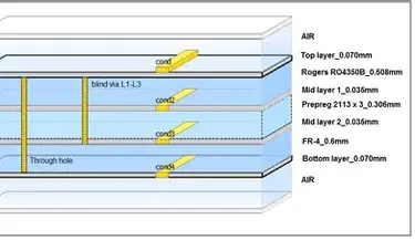
The low dissipation factor of RO4350B fundamentally reduces energy loss as electromagnetic waves propagate through the substrate. At frequencies above 1 GHz, conventional laminates exhibit increasing Df, leading to attenuation that degrades signal-to-noise ratios. RO4350B's hydrocarbon/ceramic matrix minimizes polar losses, maintaining efficiency up to 40 GHz in some configurations. Stable Dk prevents phase shifts and reflections in transmission lines, crucial for phased array antennas. Z-axis CTE matching copper's expansion reduces warpage and via cracking during thermal cycling, as per IPC-TM-650 test methods.
Signal loss in PCBs arises from conductor, dielectric, and radiation components, with dielectric loss dominating at high frequencies. RO4350B's Df value translates to insertion loss under 0.5 dB/inch at 10 GHz for microstrip lines, depending on geometry. Impedance control benefits from Dk tolerance, allowing ±5% variation in characteristic impedance for 50 Ω lines. Thermal coefficient of Dk at 50 ppm/°C from -50°C to 150°C ensures operation across automotive or aerospace temperature ranges. These mechanisms make RO4350B suitable for multilayer hybrids where FR4 cores pair with RO4350B signal layers.
RO4350B Applications in Modern Electronics
RO4350B finds extensive use in wireless infrastructure, including backhaul radios and small cells where low loss supports higher data rates. Power amplifiers benefit from its thermal properties and V-0 rating, handling RF output without hotspots. In test and measurement equipment, stable impedance enables precise vector network analyzer calibrations. Automotive radar systems at 77 GHz leverage its dimensional stability for reliable beamforming. Computing and IP infrastructure applications employ RO4350B in high-speed interconnects, reducing crosstalk in dense boards.
Military and aerospace designs incorporate RO4350B for LNBs and satcom due to its performance-cost balance. 5G base stations use it for sub-6 GHz and mmWave filters, where signal loss directly affects coverage. Multilayer power dividers and couplers maintain phase matching thanks to uniform Dk. These RO4350B applications demonstrate versatility across commercial and defense sectors.
Best Practices for Impedance Control and Signal Loss Mitigation with RO4350B
Designers achieve precise impedance control by modeling with the 3.48 Dk value and accounting for copper roughness in field solvers. Maintain trace widths within ±10% tolerance, using electrodeposited foil for low profile. For striplines, stackups with symmetric dielectrics minimize modal dispersion. Fabrication follows FR4 flows: standard drilling at 300-500 SFM with 0.002-0.004 inch/rev chip load, avoiding excessive smear due to high Tg over 280°C. Desmear uses plasma or permanganate sparingly to preserve surface integrity.
To minimize RO4350B signal loss, select low-loss foils and control etching undercuts. Multilayer bonding employs compatible prepregs, pressing at parameters per IPC-6012 guidelines for rigid boards. Bakeout before lamination reduces moisture, ensuring low insertion loss. Routing with carbide tools at under 500 SFM prevents delamination. Final finishes like ENIG support high-frequency without oxidation. These practices yield boards meeting stringent RF performance.
Conclusion
Rogers RO4350B redefines high-frequency PCB design through its optimal blend of low loss, stable properties, and ease of processing. Electrical engineers gain reliable impedance control and minimal signal loss for applications from 5G to radar. Key RO4350B properties like Dk 3.48 and Df 0.0037 enable superior performance without PTFE complexities. Adopting best practices ensures fabrication success aligned with industry standards. As high-speed systems evolve, RO4350B remains a cornerstone for innovative electronics.
FAQs
Q1: What are the main RO4350B properties for high-frequency use?
A1: RO4350B features a dielectric constant of 3.48 ± 0.05 at 10 GHz and dissipation factor of 0.0037, ensuring low signal loss and stable propagation. Low Z-axis CTE at 32 ppm/°C supports multilayer reliability. These traits make it superior to FR4 for RF circuits, per standard test methods.
Q2: How does RO4350B enable impedance control in PCB design?
A2: Tight Dk tolerance allows accurate modeling of 50 Ω microstrips and striplines with minimal frequency variation. Engineers often use the datasheet design Dk of 3.66 for stackups to compensate for process effects, yielding approximately ±5% impedance accuracy for matching networks and antennas.
Q3: What are common RO4350B applications in RF systems?
A3: RO4350B suits backhaul radios, power amplifiers, and 5G small cells due to low loss at multi-GHz bands. It excels in radar and satcom for phase-stable signals. Automotive and test equipment leverage its thermal stability for demanding environments.
Q4: How to minimize signal loss with RO4350B?
A4: Select low-profile copper, optimize trace geometry, and avoid excessive desmear to preserve Df benefits. Simulations commonly predict insertion loss below 0.5 dB/inch at 10 GHz for microstrip lines, depending on geometry. Following fabrication guidelines helps ensure performance matches datasheet expectations.


