 ALLPCB


Introduction
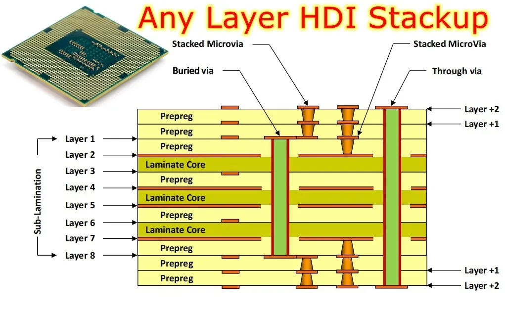
High-density interconnect (HDI) printed circuit boards have become essential for compact electronics like smartphones, medical devices, and automotive systems. FR-4, the standard glass-reinforced epoxy laminate, continues to dominate HDI manufacturing due to its balance of cost, mechanical stability, and electrical performance. Advanced FR-4 PCB HDI manufacturing techniques enable denser routing, smaller vias, and finer features while maintaining reliability under thermal and mechanical stress. These methods address the limitations of traditional through-hole designs by incorporating microvias, blind and buried vias, and multilayer build-ups. Engineers must understand these processes to optimize designs for manufacturability and performance. This article explores FR-4 PCB microvia technology, laser drilling, fine-line etching, and sequential lamination, providing factory-driven insights into their implementation.
Understanding FR-4 PCB HDI Manufacturing and Its Relevance
FR-4 PCB HDI manufacturing refers to processes that achieve high wiring density on FR-4 substrates using microvias smaller than 150 microns, trace widths below 75 microns, and complex layer stackups. This approach matters because it reduces board size by up to 50 percent compared to standard multilayers, enabling miniaturization without exotic materials. In applications demanding signal integrity and thermal management, such as 5G modules or wearables, HDI on FR-4 offers a cost-effective path to higher I/O counts. Factory production scales these techniques through precise control of drilling, plating, and lamination cycles. Compliance with IPC-2226 ensures design rules align with fabrication capabilities, minimizing defects like via opens or shorts. As component pitches shrink to 0.3 mm or less, these methods become critical for electrical engineers specifying boards.
Core Technical Principles of FR-4 PCB Microvia Technology
FR-4 PCB microvia technology relies on vias with aspect ratios up to 1:1, connecting adjacent layers without penetrating the full stackup. These vias, typically 50 to 100 microns in diameter, use dielectric thicknesses of 40 to 80 microns to maintain low capacitance. The process starts with core layers laminated with thin prepregs, followed by via formation and metallization. Reliability stems from copper plating that fills or caps the via, preventing cracks during thermal cycling. Engineers select FR-4 grades with glass transition temperatures above 170°C to withstand multiple lamination cycles. This technology supports stacked and staggered via configurations, boosting interconnect density by 4 to 6 times over conventional designs.
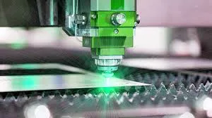
Laser drilling forms the foundation of microvia creation in FR-4. CO2 lasers at 9.3 to 10.6 microns wavelength ablate epoxy cleanly, while UV lasers at 355 nm handle finer features with minimal heat-affected zones. The process involves multiple passes for deeper vias, with galvano scanners ensuring positional accuracy within 25 microns. Post-drilling desmear removes resin residue using plasma or permanganate, preparing surfaces for electroless copper seeding. Aspect ratios beyond 0.8:1 require optimized beam profiles to avoid taper or debris. These principles enable FR-4 PCB laser drilling to achieve yields over 99 percent in high-volume production.
Fine-line etching defines traces and spaces down to 40 microns on FR-4 HDI boards. Photolithography with LDI exposure transfers patterns onto thin copper foils, typically 12 to 18 microns thick. Etchants like cupric chloride selectively remove unprotected copper, with spray systems controlling undercut to under 10 percent. Post-etch cleaning preserves line integrity, avoiding bridging or necking. This technique pairs with microvias for via-in-pad designs, where filled vias become routing nodes. Precise control of copper weight and developer strength ensures uniformity across panels.
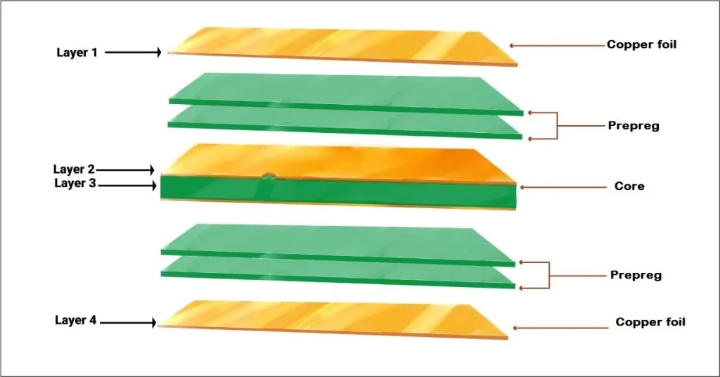
Sequential lamination builds HDI structures layer by layer, alternating dielectric application, via drilling, plating, and pressing. Starting from a core, outer layers add build-up films or prepregs, with registration pins maintaining alignment to 50 microns. Each cycle cures resins at 180 to 200°C under vacuum, minimizing voids. IPC-6016 guidelines dictate via reliability testing, including thermal shock and intermetallic growth assessments. This method supports 1+N+1 to 3+N+3 stackups, where N represents inner layers. Factory automation sequences these steps to reduce cycle times while controlling warpage through symmetric builds.
Practical Solutions and Best Practices in FR-4 HDI Production
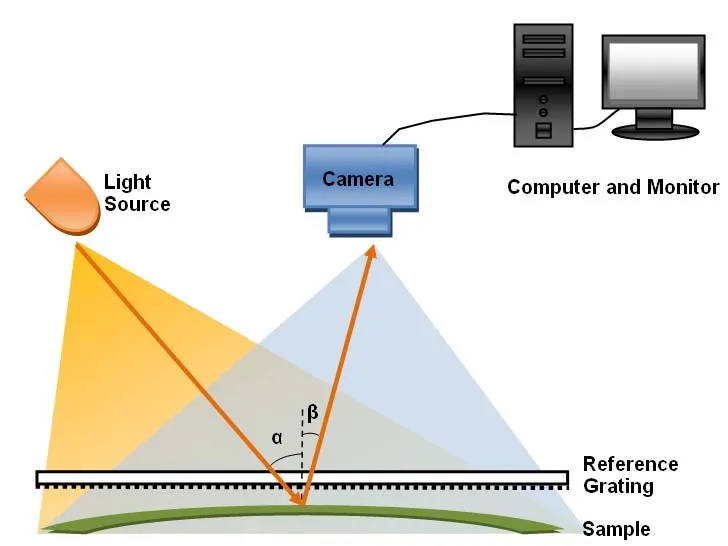
Implementing FR-4 PCB HDI manufacturing demands rigorous process controls to mitigate challenges like via barrel cracking or plating voids. Select low-CTE FR-4 variants with Z-axis expansion below 3 percent to match copper during reflow. For FR-4 PCB laser drilling, calibrate pulse energy to 50 to 100 microjoules, monitoring hole geometry via automated optical inspection. Sequential lamination benefits from carrier films that prevent outer layer distortion, peeled post-plating. Fine-line etching requires tenting soldermask over traces to shield against handling damage.
Warpage control is paramount, as asymmetric build-ups induce bow exceeding 0.75 percent. Use fixture pressing and balanced copper distribution to stay within IPC-A-600K acceptability criteria. Electrical testing post-lamination verifies continuity, with flying probe systems detecting opens in microvias. Yield optimization involves statistical process control, targeting CpK above 1.33 for critical features. Engineers should simulate thermal profiles using FEA to predict stresses in stacked vias.
For troubleshooting, inspect desmear efficacy with cross-sectioning if via reliability fails. Common issues like laser taper arise from defocused beams, resolved by real-time autofocus. Fine-line shorts trace to over-etching, countered by endpoint detection in chemistry baths. Sequential build registration errors demand enhanced fiducials and optical alignment.
Key Challenges and Mitigation Strategies
HDI on FR-4 faces thermal mismatch between epoxy and copper, leading to via fatigue after 1000 cycles. Mitigation includes filled vias with electroplated copper, expanding less than epoxy. Laser drilling debris can cause resin smears, addressed by optimized suction and plasma cleaning. Fine-line etching undercuts thin foils, so use pulse plating for uniform deposition. Sequential lamination risks delamination if moisture exceeds 0.25 percent, necessitating bake-out protocols per JEDEC J-STD-020E.
Panel-level processing scales production, but edge effects demand beveling for uniform etching. Signal integrity improves with controlled impedance stacks, targeting 50 ohms for microstrip lines.
Conclusion
Advanced FR-4 PCB HDI manufacturing techniques like microvia technology, laser drilling, fine-line etching, and sequential lamination enable compact, reliable boards for demanding applications. These processes demand precise control to balance density with yield and durability. Electrical engineers benefit from aligning designs with factory capabilities, referencing standards like IPC-2226 and IPC-6016. As electronics shrink further, FR-4 HDI remains a versatile choice, driving innovation without excessive costs. Mastering these methods ensures robust performance in production.
FAQs
Q1: What is FR-4 PCB HDI manufacturing?
A1: FR-4 PCB HDI manufacturing involves building high-density boards using microvias, fine traces, and sequential layers on standard FR-4 laminates. Key steps include laser drilling for vias under 150 microns, plating, and multiple lamination cycles. This achieves routing densities up to 200,000 nets per square decimeter while controlling costs. Factories emphasize process repeatability to meet IPC class 3 reliability.
Q2: How does FR-4 PCB laser drilling support microvia technology?
A2: FR-4 PCB laser drilling uses CO2 or UV lasers to create precise microvias with minimal heat damage. The process ablates epoxy selectively, followed by desmear and plating for electrical connectivity. It enables stacked configurations in sequential builds, improving I/O escape. Best practices include pulse optimization to avoid taper, ensuring aspect ratios up to 1:1.
Q3: What are the benefits of FR-4 PCB sequential lamination?
A3: FR-4 PCB sequential lamination allows layer-by-layer construction, supporting blind, buried, and stacked vias for complex HDI stackups. It minimizes board thickness while maximizing density, ideal for BGA fanout. Alignment controls and symmetric builds prevent warpage. This technique aligns with IPC-6016 for qualification, enhancing thermal and mechanical stability.
Q4: Why is FR-4 PCB fine-line etching critical for HDI designs?
A4: FR-4 PCB fine-line etching produces traces and spaces below 50 microns, enabling dense routing around microvias. Thin copper foils and advanced lithography ensure clean profiles without undercuts. It supports via-in-pad for space savings. Process controls like etch endpoint detection maintain uniformity across panels.
References
IPC-2226 — Sectional Design Standard for High Density Interconnects. IPC.
IPC-6016D — Qualification and Performance Specification for High Density Interconnect (HDI) Printed Boards. IPC.
IPC-A-600K — Acceptability of Printed Boards. IPC, 2020.
JEDEC J-STD-020E — Moisture/Reflow Sensitivity Classification. JEDEC, 2014.





