 ALLPCB


Introduction
Flying probe testing has emerged as a key method in printed circuit board development, particularly when engineers need reliable validation during the prototype phase. This approach supports rapid prototyping by allowing electrical verification without the need for dedicated fixtures. It aligns well with quick turn PCB testing workflows, where time to first article inspection directly influences overall project timelines. Engineers rely on it for prototype validation because it provides detailed feedback on connectivity and component integrity early in the design cycle. Early design verification through this technique helps identify issues before they propagate into production, reducing the risk of costly revisions later.
What Is Flying Probe Testing and Why It Matters
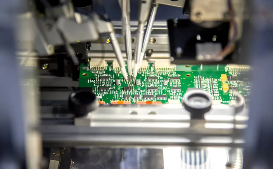
Flying probe testing uses movable probes that contact specific points on a printed circuit board to perform electrical measurements. Unlike fixed-fixture methods, the probes move independently across the board surface under computer control, enabling tests on a wide range of board layouts. This flexibility proves especially valuable during rapid prototyping, when designs frequently change and fixture fabrication would introduce delays. Quick turn PCB testing benefits from the minimal setup time, as programs can be generated directly from design files. Prototype validation becomes more efficient because the same equipment can handle multiple iterations without hardware changes. Early design verification gains accuracy through repeatable measurements of continuity, isolation, and passive component values.
Technical Principles of Flying Probe Testing
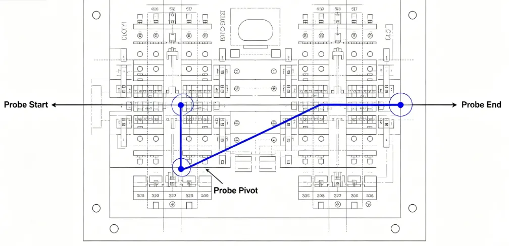
The process begins with importing board design data to generate a test program that maps nets and test points. Probes then travel along optimized paths to make sequential contact with pads or vias. Electrical tests include continuity checks to confirm intended connections and isolation tests to detect unintended shorts between nets. Additional measurements cover resistance, capacitance, and inductance where applicable, providing quantitative data on component performance. Probe positioning accuracy supports fine-pitch designs common in modern prototypes. The method follows established practices outlined in IPC-9252B for electrical testing of unpopulated printed boards, ensuring consistent coverage and traceability of results.
Test coverage depends on accessible points and probe count, typically allowing comprehensive checks on boards up to several hundred nets. Data logging records pass or fail status for each test, along with measured values, which supports detailed analysis during prototype validation. Engineers can correlate failures back to specific locations on the board layout for targeted debugging. This structured approach delivers objective evidence of board integrity without requiring physical fixtures.
Practical Applications and Best Practices for Prototype Validation
Engineers integrate flying probe testing into the design review process after initial fabrication to confirm that the manufactured board matches the intended schematic and layout. Best practices include defining test points during the design stage to maximize coverage while respecting spacing rules. Programs should be reviewed for completeness before running the first test on a new prototype batch. Quick turn PCB testing workflows benefit when test results are available within hours of board arrival, enabling immediate feedback loops. Early design verification improves when measurements are compared against expected tolerances derived from component datasheets and circuit simulations.
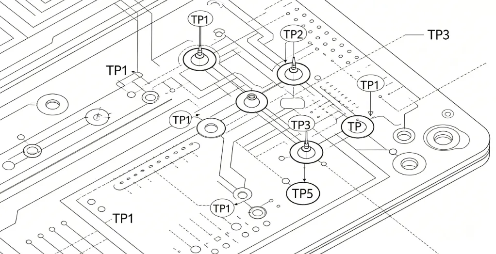
Documentation of test parameters and results aids traceability, which aligns with quality expectations in IPC-6012E for qualification of rigid printed boards. Teams often run a subset of tests focused on critical nets during initial iterations, expanding coverage as the design stabilizes. This phased approach balances thoroughness with the speed required in rapid prototyping environments.
Benefits for Rapid Prototyping and Quick Turn PCB Testing
The absence of custom fixtures eliminates lead times associated with mechanical tooling, allowing testing to begin as soon as boards arrive. Multiple board revisions can be evaluated on the same equipment, supporting iterative refinement without additional capital investment. Measurement repeatability helps distinguish between manufacturing variations and design issues during prototype validation. Engineers obtain quantitative data that supports root-cause analysis, accelerating resolution of connectivity or component problems. Early design verification through this method reduces the likelihood of discovering defects after assembly or in functional testing.
The technique scales effectively from single boards to small batches, fitting naturally into quick turn PCB testing schedules. Data outputs integrate with existing quality systems, providing records that support compliance efforts without additional manual logging.
Conclusion
Flying probe testing delivers a practical solution for electrical verification in the prototype stage by combining flexibility with detailed measurement capability. Its role in rapid prototyping stems from reduced setup requirements and strong support for iterative design changes. When applied consistently, it strengthens prototype validation and early design verification processes. Teams that incorporate it into their workflows gain clearer insight into board performance ahead of volume production.
FAQs
Q1: What advantages does flying probe testing for rapid prototyping offer compared with traditional methods?
A1: Flying probe testing for rapid prototyping eliminates the need for custom fixtures, enabling fast program generation from design files and immediate testing of new board iterations. This supports quick identification of connectivity issues and component value deviations during early development stages. Engineers benefit from repeatable measurements that aid prototype validation without extended lead times.
Q2: How does quick turn PCB testing integrate with flying probe methods?
A2: Quick turn PCB testing uses flying probe equipment to deliver electrical results within hours of board receipt, fitting compressed development schedules. The process verifies continuity, isolation, and basic component parameters across accessible points. Results feed directly into design reviews, supporting timely adjustments before further fabrication.
Q3: Why is flying probe testing effective for prototype validation?
A3: Flying probe testing provides quantitative data on electrical integrity that confirms whether a manufactured prototype matches design intent. It detects opens, shorts, and out-of-tolerance values without requiring dedicated hardware. This objective feedback accelerates prototype validation cycles and informs targeted design refinements.
Q4: In what ways does early design verification benefit from flying probe testing?
A4: Early design verification gains from flying probe testing through detailed mapping of net connectivity and passive component performance on the physical board. Measurements highlight discrepancies between simulation and reality at an early stage. The method supports systematic review of critical circuits before committing to assembly or higher-volume runs.
References
IPC-6012E — Qualification and Performance Specification for Rigid Printed Boards. IPC, 2017
IPC-A-600K — Acceptability of Printed Boards. IPC, 2020
IPC-9252B — Requirements for Electrical Testing of Unpopulated Printed Boards. IPC, 2016





