Via design in PCBs is a critical factor in ensuring both performance and reliability in modern electronics. Whether you're working on high-speed circuits, thermal management, or multilayer boards, the way vias are implemented can make or break your design. In this comprehensive guide, we’ll explore how to optimize PCB via design, covering via types, via stitching, thermal vias, and high-speed via design techniques. Let’s dive into the details to help you create efficient, reliable, and high-performing printed circuit boards.
What Are Vias in PCB Design?
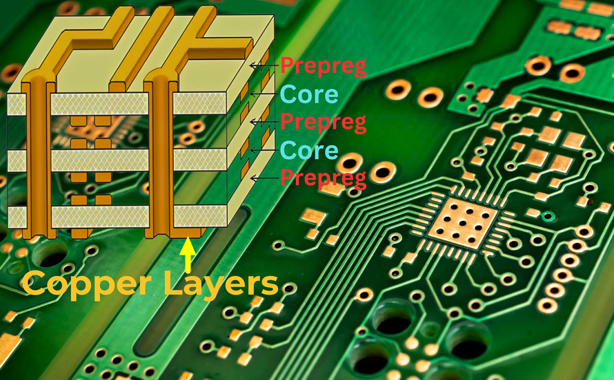
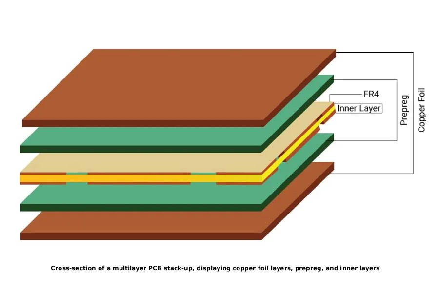
Vias, short for Vertical Interconnect Access, are small conductive pathways that connect different layers of a printed circuit board. These tiny holes, often filled or plated with conductive material like copper, allow electrical signals and power to travel between layers in multilayer PCBs. Without vias, signals would be confined to a single layer, severely limiting the complexity and functionality of modern electronics.
However, not all vias are created equal. Poorly designed vias can introduce signal loss, electromagnetic interference (EMI), or thermal issues. Optimizing via design is essential for ensuring signal integrity, managing heat, and maintaining the overall reliability of your PCB. In the sections below, we’ll break down the key aspects of PCB via design and provide actionable tips for success.
Types of Vias in PCB Design
Understanding the different types of vias is the first step in optimizing your PCB layout. Each type serves a specific purpose and comes with its own set of advantages and challenges. Let’s explore the most common via types used in PCB design.
- Through-Hole Vias: These vias extend through the entire thickness of the PCB, connecting the top and bottom layers. They are the most common and easiest to manufacture but take up more space and may not be ideal for high-density designs.
- Blind Vias: Blind vias connect an outer layer to an inner layer without passing through the entire board. They save space and are often used in high-density interconnect (HDI) designs, though they are more expensive to fabricate.
- Buried Vias: These vias connect internal layers without reaching the outer surfaces of the PCB. They are invisible from the outside and are useful for compact designs but add complexity and cost to manufacturing.
- Microvias: Microvias are small-diameter vias, typically less than 150 micrometers, used in HDI boards. They enable finer routing and are often laser-drilled for precision, making them ideal for compact, high-speed designs.
- Thermal Vias: Specifically designed to transfer heat away from components, thermal vias are often placed under heat-generating parts like power ICs. They connect to large copper planes to dissipate heat effectively.
Key Considerations for PCB Via Design
When designing vias for a PCB, several factors must be considered to ensure optimal performance and reliability. Let’s look at the most important aspects to keep in mind.
1. Via Size and Aspect Ratio
The size of a via, including its diameter and depth, plays a significant role in its performance. Smaller vias reduce parasitic capacitance and inductance, which is crucial for high-speed signals. However, smaller vias are harder to manufacture and may have higher resistance. A common rule of thumb is to maintain an aspect ratio (depth-to-diameter) of less than 10:1 to ensure reliable plating during fabrication. For example, a via with a depth of 1.6 mm should have a minimum diameter of 0.16 mm.
2. Placement and Spacing
Via placement affects signal routing and board density. Placing vias too close to each other can cause manufacturing defects or crosstalk in high-speed designs. A spacing of at least 0.5 mm between vias is often recommended for standard designs, though this may vary based on the board’s complexity and manufacturing capabilities.
3. Material and Plating
Vias are typically plated with copper to ensure conductivity, but the quality of plating can impact reliability. Poor plating can lead to voids or cracks, causing electrical failures over time. Ensure that your design adheres to industry standards for plating thickness, often around 25 micrometers for reliable performance.
Via Stitching: Enhancing Signal Integrity and EMI Control
Via stitching is a technique used to connect large copper planes, such as ground or power planes, across multiple layers of a PCB. By placing multiple vias in a grid or pattern around the edges of these planes, via stitching helps to reduce EMI, improve signal integrity, and enhance thermal performance.
Benefits of Via Stitching
- Reduced EMI: Stitching vias create a low-impedance path for return currents, minimizing electromagnetic interference in high-frequency designs.
- Improved Signal Integrity: By providing a consistent reference plane, stitching vias help maintain stable signal paths, reducing noise and reflections.
- Better Heat Distribution: Stitching vias can also act as thermal conduits, spreading heat across layers to prevent hotspots.
Best Practices for Via Stitching
For effective via stitching, place vias at regular intervals, typically every 1/8th of the wavelength of the highest frequency signal on the board. For a 2.4 GHz signal, with a wavelength of approximately 125 mm in air, this translates to a via spacing of about 15 mm. However, closer spacing (e.g., 5-10 mm) may be necessary for very high-speed designs to ensure optimal performance. Additionally, avoid placing stitching vias too close to signal traces to prevent unintended coupling.
Thermal Vias: Managing Heat in High-Power Designs
Thermal management is a critical concern in PCB design, especially for applications involving high-power components like LEDs, power amplifiers, or processors. Thermal vias are an effective solution for dissipating heat by connecting heat-generating components to large copper planes or heat sinks on other layers.
Designing Thermal Vias
To maximize heat transfer, thermal vias should have a larger diameter (e.g., 0.3-0.5 mm) compared to signal vias. They are often arranged in a grid pattern under the component, with 8-16 vias per square centimeter for high-power devices dissipating 5-10 watts of heat. Filling thermal vias with conductive epoxy or copper can further improve thermal conductivity, though this increases manufacturing costs.
Placement Tips
Place thermal vias directly under or near the heat source for maximum efficiency. Connect them to a large copper plane on the opposite layer to spread heat evenly. Avoid placing other components or traces near thermal vias to prevent interference with heat dissipation paths.
High-Speed Via Design: Ensuring Signal Integrity
In high-speed PCB designs, vias can introduce significant signal integrity issues if not optimized. At frequencies above 1 GHz, vias act as impedance discontinuities, causing reflections, crosstalk, and signal loss. Here’s how to design vias for high-speed applications.
Minimize Via Stub Length
A via stub is the unused portion of a via that extends beyond the connected layers. Long stubs can resonate at high frequencies, degrading signal quality. For a 5 GHz signal, a stub length longer than 0.5 mm can cause noticeable reflections. Use back-drilling to remove unused via stubs or opt for blind vias to eliminate stubs entirely.
Use Differential Vias for High-Speed Pairs
In differential signaling, such as USB 3.0 or PCIe, vias for differential pairs should be placed symmetrically to maintain consistent impedance. A typical differential impedance target is 100 ohms, and via spacing should match the trace spacing (often 0.2-0.3 mm) to avoid skew and crosstalk.
Optimize Return Paths
High-speed signals require a continuous return path to minimize loop inductance. Place ground vias near signal vias to provide a low-impedance return path. For example, in a 10-layer PCB with a 2.5 GHz signal, placing a ground via within 0.5 mm of each signal via can reduce loop inductance by up to 50%.
Common Mistakes in PCB Via Design
Even experienced designers can make mistakes when it comes to via design. Avoiding these pitfalls can save time and prevent costly redesigns.
- Overlooking Via Current Capacity: Vias have limited current-carrying capacity. A 0.3 mm diameter via can typically handle about 1-2 amps. Use multiple vias or larger diameters for high-current paths.
- Ignoring Manufacturing Constraints: Not all via sizes or types are supported by every manufacturer. Always check design rules to avoid fabrication issues.
- Neglecting Thermal Expansion: Vias can crack due to thermal expansion if not designed with adequate clearance. Ensure via pads are large enough (e.g., 0.2 mm larger than the via diameter) to accommodate stress.
Conclusion: Mastering Via Design for Better PCBs
Via design in PCBs is more than just connecting layers—it’s about optimizing performance, ensuring reliability, and meeting the demands of modern electronics. By understanding via types, implementing via stitching for EMI control, using thermal vias for heat management, and refining high-speed via design, you can create robust and efficient PCB layouts. Pay attention to details like via size, placement, and manufacturing constraints to avoid common pitfalls and achieve the best results.
With the right approach to PCB via design, you’ll be well-equipped to tackle complex projects, from high-speed digital circuits to power-intensive applications. Keep these tips and techniques in mind as you design your next board, and watch your designs reach new levels of performance and reliability.
 ALLPCB


