Are you struggling with PCB layout issues like signal integrity problems, ground loops, or noise interference? Troubleshooting a printed circuit board (PCB) can be challenging, but with a systematic approach and the right tools, you can identify and resolve these issues efficiently. In this comprehensive guide, we’ll walk you through a step-by-step process for PCB troubleshooting, covering common problems such as power distribution issues, design rule violations, and more. By using advanced software solutions, you can streamline the debugging process and ensure your PCB design performs flawlessly.
Whether you’re an experienced engineer or a beginner in PCB design, this blog will provide actionable tips and techniques for addressing signal integrity issues, ground loops, noise problems, and other layout challenges. Let’s dive into the world of PCB debugging and layout review to help you achieve a reliable and high-performing design.
Why PCB Troubleshooting Matters
PCBs are the backbone of modern electronics, connecting components and ensuring proper functionality. However, even a small error in the layout can lead to major issues like signal distortion, power failures, or electromagnetic interference (EMI). These problems can cause your device to malfunction, leading to costly redesigns or delays in production. Effective PCB troubleshooting is essential to catch these issues early, saving time and resources while ensuring the reliability of your product.
Common PCB layout issues include signal integrity problems, where high-speed signals degrade due to impedance mismatches (often around 50 ohms for standard designs); ground loops, which introduce unwanted noise; and power distribution problems, where uneven voltage delivery affects performance. By adopting a systematic approach and leveraging software tools, you can pinpoint the root causes of these issues and fix them before they escalate.
Common PCB Layout Issues and Their Impact
Before diving into troubleshooting techniques, it’s important to understand the most common PCB layout issues and how they affect performance. Here’s a breakdown of the key challenges engineers face:
- Signal Integrity Issues: High-speed designs often suffer from signal degradation due to crosstalk, reflections, or impedance mismatches. For example, a mismatch in a 100 MHz signal line can cause reflections, leading to data errors.
- Ground Loops: These occur when multiple ground paths create a loop, allowing noise to interfere with sensitive signals. This is common in mixed-signal designs where analog and digital grounds are not properly separated.
- Noise Problems: EMI and RF interference can disrupt signal clarity, especially in densely packed boards or near high-power components.
- Power Distribution Problems: Uneven voltage distribution or insufficient decoupling capacitors can lead to voltage drops, often below the required 3.3V or 5V for microcontrollers, causing erratic behavior.
- Design Rule Violations: Failing to adhere to manufacturing constraints, such as minimum trace widths (e.g., 6 mils for standard processes), can result in fabrication errors.
Understanding these issues is the first step in effective PCB debugging. With the right tools and techniques, you can address each problem systematically.
A Systematic Approach to PCB Troubleshooting
Troubleshooting a PCB layout requires a structured process to identify and resolve issues efficiently. Below, we outline a step-by-step approach to PCB debugging that covers everything from layout review to final testing. This method works for both simple and complex designs, ensuring you don’t miss critical problems.
Step 1: Conduct a Thorough Layout Review
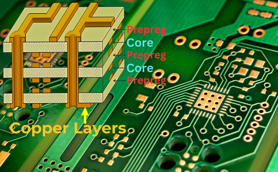
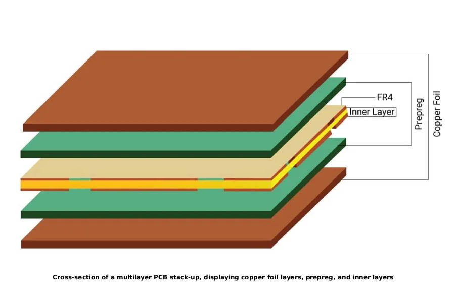
Start by reviewing your PCB layout before manufacturing. A detailed layout review can catch potential issues like design rule violations or improper component placement. Use software tools to simulate your design and check for errors in trace routing, component spacing, and layer stackup. For instance, ensure that high-speed traces are kept short (under 1 inch for signals above 100 MHz) to minimize signal delay and reflections.
Focus on key areas such as:
- Trace spacing to avoid crosstalk (maintain at least 3x the trace width for high-speed signals).
- Ground plane continuity to prevent ground loops.
- Power rail routing to ensure consistent voltage delivery across the board.
Step 2: Use Software for Design Rule Checks (DRC)
Modern PCB design software includes built-in Design Rule Check (DRC) features to flag violations automatically. These tools analyze your layout against predefined rules, such as minimum trace widths (e.g., 8 mils for power traces) or clearance distances (e.g., 10 mils between traces). Running a DRC early in the design process helps catch issues before they become costly mistakes during fabrication.
Software can also highlight potential signal integrity issues by simulating impedance mismatches or identifying areas prone to EMI. By addressing these violations upfront, you reduce the risk of noise problems and power distribution issues later on.
Step 3: Simulate Signal Integrity and Power Distribution
Signal integrity issues and power distribution problems are often invisible until the board is powered on. To avoid surprises, use simulation tools within your PCB software to model signal behavior and power delivery. For example, simulate a high-speed signal at 500 MHz to check for reflections or crosstalk. If the impedance deviates from the target (e.g., 50 ohms), adjust the trace width or dielectric material to match.
For power distribution, simulate voltage drops across the board. If a critical component receives less than 3.3V due to IR drop, consider adding thicker traces (e.g., 20 mils) or more decoupling capacitors (e.g., 0.1 μF near IC pins) to stabilize the supply.
Step 4: Test for Ground Loops and Noise Problems
Ground loops and noise problems often appear during testing. To identify ground loops, use an oscilloscope to measure voltage differences between ground points. A difference of more than 50 mV indicates a potential loop. Fix this by ensuring a single, continuous ground plane or by separating analog and digital grounds with a star-point connection.
For noise issues, look for EMI sources like switching regulators or nearby RF components. Adding shielding or rerouting sensitive traces away from noise sources (at least 100 mils apart) can help. Software tools can also simulate EMI hotspots, guiding you to areas needing attention.
Step 5: Debug and Iterate
Once the PCB is fabricated, test it under real-world conditions. Use multimeters to check voltage levels at key points (e.g., ensuring 5V at power pins) and oscilloscopes to monitor signal waveforms for distortion. If issues persist, revisit your layout in the software, make adjustments, and simulate again. PCB debugging often requires multiple iterations to achieve optimal performance.
Leveraging [Software] for PCB Troubleshooting
Advanced software plays a crucial role in PCB troubleshooting, offering tools for layout review, simulation, and debugging. With [Software], you can streamline the process of identifying signal integrity issues, ground loops, and power distribution problems. Here’s how [Software] supports a systematic approach to PCB debugging:
- Automated Design Rule Checks: Quickly identify violations like insufficient clearance or incorrect trace widths, ensuring compliance with manufacturing standards.
- Signal Integrity Analysis: Simulate high-speed signals (up to 1 GHz) to detect crosstalk or reflections, allowing you to adjust trace lengths or terminations before fabrication.
- Power Integrity Simulation: Model voltage distribution to ensure all components receive stable power, preventing issues like voltage drops below 3.3V.
- EMI and Noise Prediction: Identify potential noise sources and suggest layout adjustments, such as increasing ground plane coverage or adding vias for better grounding.
Using [Software], you can visualize complex issues in an intuitive interface, making it easier to address design rule violations and optimize your layout. This reduces the need for costly prototypes and accelerates the debugging process.
Best Practices for Preventing PCB Layout Issues
While troubleshooting is essential, preventing issues during the design phase is even better. Here are some best practices to minimize signal integrity issues, ground loops, and other common problems:
- Plan Your Ground Planes: Use a solid ground plane on one layer to provide a low-impedance return path, reducing the risk of ground loops. Avoid splitting the ground plane unless necessary for analog-digital separation.
- Optimize Trace Routing: Keep high-speed traces short and direct, maintaining consistent impedance (e.g., 50 ohms for RF signals). Route sensitive traces away from power lines to avoid noise coupling.
- Use Decoupling Capacitors: Place capacitors (e.g., 0.01 μF and 0.1 μF) near IC power pins to filter noise and stabilize voltage levels.
- Follow Design Guidelines: Adhere to manufacturer design rules, such as minimum via sizes (e.g., 12 mils) and trace spacing, to avoid fabrication errors.
- Simulate Early and Often: Run simulations at every stage of the design process to catch potential issues like power distribution problems before they manifest.
By incorporating these practices into your workflow, you can reduce the need for extensive PCB troubleshooting and achieve a more reliable design from the start.
Case Study: Resolving a Signal Integrity Issue
To illustrate the power of systematic troubleshooting, consider a real-world example. An engineer working on a high-speed communication board noticed data errors at 200 MHz. Using [Software], they simulated the signal paths and discovered an impedance mismatch—traces were designed for 75 ohms instead of the required 50 ohms. By adjusting the trace width from 10 mils to 15 mils and adding termination resistors, the issue was resolved. Post-fabrication testing confirmed clean signal waveforms with no reflections.
This case highlights the importance of simulation and software tools in identifying and fixing signal integrity issues before they impact performance. A systematic approach, combined with the right tools, ensures success even in complex designs.
Conclusion: Master PCB Troubleshooting with the Right Tools
Troubleshooting PCB layout issues doesn’t have to be overwhelming. By following a systematic approach—starting with layout review, using DRC tools, simulating signal and power integrity, testing for noise, and iterating as needed—you can address common problems like signal integrity issues, ground loops, and power distribution problems. With advanced software like [Software], the process becomes even more efficient, offering powerful features for simulation, analysis, and debugging.
At ALLPCB, we’re committed to supporting engineers with resources and tools to create reliable, high-performance designs. Whether you’re dealing with design rule violations or noise problems, a structured PCB debugging process will help you achieve success. Implement the tips and techniques shared in this guide to streamline your workflow and build better PCBs every time.
 ALLPCB


