 ALLPCB


Introduction
Wearable fitness devices, such as fitness trackers and smartwatches, demand highly reliable PCB assemblies due to their compact size and constant exposure to motion, sweat, and temperature fluctuations. PCB assembly defects wearables can compromise sensor accuracy, battery life, and overall functionality, leading to field failures that erode user trust. Engineers troubleshooting these issues must focus on high-density surface-mount technology processes tailored for small form factors. Common challenges include soldering issues fitness tracker experiences during reflow and component placement errors PCB setups face with tiny passives. This article provides practical guidance on identifying, diagnosing, and resolving these defects using industry-standard inspection criteria. By understanding root causes and implementing targeted fixes, assembly teams can enhance yield and reliability.

Why PCB Assembly Defects Matter in Wearable Fitness Devices
Wearables operate in harsh environments, where even minor assembly flaws can trigger intermittent faults during activities like running or swimming. Defects such as poor solder joints accelerate under mechanical stress from flexing straps or body movements, reducing mean time between failures. In high-volume production, these issues inflate rework costs and delay time-to-market for fitness devices. Component placement errors PCB directly impact signal integrity for heart rate sensors or accelerometers, causing data inaccuracies that users notice immediately. Adhering to standards like IPC-A-610 ensures assemblies meet Class 2 or Class 3 requirements for consumer electronics reliability. Proactive defect management thus supports scalable manufacturing for fitness wearables.
Common Types of PCB Assembly Defects in Wearables
Soldering Defects
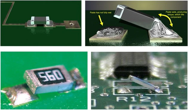
Soldering issues fitness tracker assemblies often manifest as bridges, where excess solder paste connects adjacent pads, shorting signals in dense layouts. Cold solder joints appear dull and cracked, failing to form a metallurgical bond due to insufficient heat or contamination. Solder balls, small spheres detached during reflow, pose risks of electrical shorts under vibration. Voids in solder joints, visible via X-ray, trap gases and weaken mechanical strength in battery-connected circuits. Tombstoning lifts one end of chip components like 0201 resistors, common in wearables from uneven reflow heating. These defects account for a significant portion of failures in small form factor electronics.
Component Placement Errors
Component placement errors PCB arise frequently in wearables due to the precision needed for micro-components under 0.4 mm pitch. Misalignment shifts parts off pads by more than 25% of lead width, disrupting solder wicking and joint formation. In pick-and-place processes, feeder jams or vision system offsets exacerbate issues with fine-pitch QFNs used for processors. Gravitational pull during reflow worsens placement drift on vertical orientations. These errors lead to open circuits in power rails, halting device boot-up. Flexible substrates in wearables amplify misalignment from warpage during handling.
Other Prevalent Defects
Warpage exceeds allowable limits on thin flex-rigid boards, pulling components away from pads during reflow. Contamination from flux residues causes dendritic growth over time, especially in humid fitness tracker environments. Pad lifting occurs when excessive heat delaminates copper from the substrate in multilayer stacks. Head-in-pillow defects trap components atop unmelted solder paste, mimicking good joints visually but failing electrically. Delamination between layers compromises via integrity in HDI designs common for wearables.
Root Causes and Mechanisms Behind These Defects
Soldering defects stem from reflow profile mismatches, where peak temperatures fall below 220°C for lead-free alloys, preventing full paste activation. Excessive solder volume from stencil aperture misalignment creates bridges, as paste collapses during melting. Component placement errors PCB result from mechanical tolerances in nozzles exceeding 50 μm, combined with board vibration on conveyors. Warpage mechanisms involve coefficient of thermal expansion mismatches between copper and substrate, bowing boards beyond 0.75% per IPC criteria. Contamination introduces ionic residues that migrate under bias, accelerating corrosion in sweat-exposed devices. Human factors, like improper handling, introduce ESD damage to sensitive sensors.
In fitness trackers, moisture sensitivity plays a role, as per JEDEC J-STD-020 guidelines, where un-baked components absorb humidity, popping during reflow and causing voids. Uneven heating gradients across small boards lead to tombstoning, as surface tension pulls lighter ends upward first. Process variations, such as stencil wear reducing aperture volume by 10–20%, contribute to insufficient wetting. These interconnected causes demand holistic process controls for wearable assemblies.
Troubleshooting Methods for PCB Assembly Defects
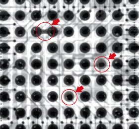
Visual inspection under 10x magnification reveals bridges, misalignment, and cold joints per IPC-A-610 acceptance levels. Automated optical inspection scans for placement offsets exceeding 0.1 mm, flagging 95% of defects early. X-ray analysis detects voids and bridging under components, essential for BGAs in wearables. Electrical testing with flying probes verifies continuity, isolating opens from placement errors. Thermal profiling during reflow confirms soak and peak zones align with paste specifications. Cross-sectioning samples provides microstructural insights into joint integrity.
For soldering issues fitness tracker prototypes face, AOI combined with SIR testing assesses flux cleanliness. Component placement errors PCB require fiducial mark verification on panels to calibrate pick-and-place accuracy. Warped boards benefit from shadow moiré metrology to quantify bow before assembly. In-circuit testing simulates operational stresses, catching intermittent faults from poor joints. Rework follows IPC-7711/7721 procedures, using hot air for precise removal without pad damage.
Best Practices to Prevent and Mitigate Defects
Optimize stencil design with 1:1 aperture-to-pad ratios and trapezoidal walls to control paste release on fine pitches. Validate reflow ovens with thermocouples at multiple zones, ensuring ramp-up rates below 3°C/s to avoid thermal shock. Implement board support fixtures to minimize warpage during placement and reflow, targeting under 0.5% deflection. Use nitrogen atmospheres to reduce oxidation, cutting solder balls by promoting wetting. Calibrate pick-and-place vision systems daily, achieving <30 μm accuracy for 01005 components.
Pre-assembly baking at 125°C for 24 hours per JEDEC J-STD-020 prevents moisture-induced defects. Solder paste inspection via SPI verifies volume uniformity within 10%. Post-reflow, enforce AOI reject limits and manual verification for Class 3 assemblies. Process data analytics track defect Pareto charts, prioritizing top issues like bridges. Operator training on J-STD-001 soldering requirements ensures consistent hand-assembly for prototypes.
Troubleshooting Case Study: Fitness Tracker Power Failure
A batch of fitness trackers exhibited random shutdowns traced to open joints on power management ICs. Initial AOI missed subtle misalignment due to 0402 capacitor shifts from feeder misalignment. X-ray confirmed non-wet opens, with solder only on pads. Root cause analysis revealed stencil thickness variation from cleaning cycles, reducing paste height. Reflow profiles showed inadequate pre-heat, causing flux burnout.
Corrective actions included stencil laser verification and profile tweaks to extend soak by 30 seconds. Baking schedules were enforced, and fixtures added for board planarity. Yield improved from 85% to 98%, with no field returns post-fix. This case underscores integrating IPC-A-610 inspections with process SPC for wearables.
Conclusion
Addressing PCB assembly defects wearables requires a systematic approach from design to test, focusing on soldering issues fitness tracker and component placement errors PCB. Key to success lies in standards-driven inspections, precise process controls, and data-driven refinements. Engineers benefit from tools like AOI and X-ray to catch issues early, while best practices prevent recurrence. Reliable assemblies ensure fitness devices perform consistently, meeting user expectations for durability. Implementing these strategies minimizes downtime and supports innovation in compact electronics.
FAQs
Q1: What are the most common soldering issues fitness tracker PCBs face during assembly?
A1: Soldering issues fitness tracker assemblies include bridges from excess paste, cold joints from poor heating, and tombstoning from uneven reflow. These arise in high-density layouts with small components. Troubleshooting involves AOI for visuals and X-ray for subsurface flaws. Prevention uses optimized profiles per J-STD-001 and nitrogen reflow. Regular stencil maintenance cuts defect rates significantly.
Q2: How do component placement errors PCB impact wearable reliability?
A2: Component placement errors PCB cause opens and weak joints, leading to signal loss in sensors. Misalignment over 25% pad width disrupts wetting in wearables. Vision systems detect offsets, while fixtures stabilize boards. Design panels with fiducials aids accuracy. Adhering to IPC-A-610 Class 2 criteria ensures robust performance under flex.
Q3: What steps troubleshoot warpage in PCB assembly defects wearables?
A3: Warpage in PCB assembly defects wearables stems from CTE mismatch, measured via shadow moiré. Inspect pre-reflow bow against 0.75% limits. Use low-stress laminates and support pins during processing. Thermal profiling prevents excessive ramp rates. Post-bake flattening restores planarity for reliable joints.
Q4: How prevent voids in solder joints for fitness devices?
A4: Voids form from trapped flux gases or moisture in reflow. Bake components per JEDEC J-STD-020 before assembly. Optimize profiles with longer soaks for outgassing. Nitrogen reduces oxidation-induced voids. X-ray verifies <25% area voids per IPC-A-610. These steps enhance thermal cycling reliability.
References
IPC-A-610H — Acceptability of Electronic Assemblies. IPC, 2019
J-STD-001G — Requirements for Soldered Electrical and Electronic Assemblies. IPC, 2011
JEDEC J-STD-020E — Moisture/Reflow Sensitivity Classification of Nonhermetic Surface Mount Devices. JEDEC, 2014


