In the world of electronics, managing heat in printed circuit boards (PCBs) is crucial for ensuring performance and longevity. Poor thermal management can lead to component failure, reduced efficiency, and costly redesigns. So, how do you master PCB thermal management design to enhance durability? The answer lies in strategic design techniques like using thermal vias, optimizing heat sink placement, applying effective cooling methods, and leveraging thermal simulation tools.
In this comprehensive guide, we'll dive deep into these strategies, offering practical tips and actionable insights for engineers and designers. Whether you're working on high-power applications or compact devices, these PCB cooling techniques will help you build reliable and durable boards. Let’s explore the key methods to keep your PCBs cool and performing at their best.
Why Thermal Management Matters in PCB Design
Heat is the enemy of electronics. As components like processors, power transistors, and LEDs operate, they generate heat that can degrade performance or cause outright failure if not managed properly. Excessive temperatures can lead to thermal expansion, warping, and even solder joint failures. Studies show that for every 10°C rise in temperature, the lifespan of electronic components can be halved. This makes PCB thermal management design a critical factor in ensuring durability and reliability.
Effective thermal management not only protects components but also improves system efficiency. By maintaining optimal operating temperatures, you can prevent throttling in high-performance devices and ensure consistent functionality. Let’s break down the core techniques that can help you achieve this.
1. Leveraging Thermal Vias for Efficient Heat Dissipation
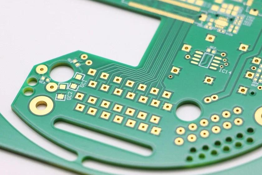
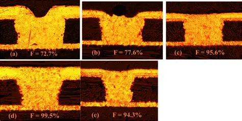
One of the most effective ways to manage heat in a PCB is through the use of thermal vias PCB structures. Thermal vias are small, plated-through holes that transfer heat from one layer of the board to another, typically from a hot component on the surface to a heat-dissipating layer or plane beneath.
How Thermal Vias Work: These vias act as conduits for heat, allowing it to move away from critical components to areas where it can be dissipated more effectively, such as a copper plane or an external heat sink. For example, in a multilayer PCB, thermal vias placed under a high-power IC can channel heat to a ground plane, reducing the component’s junction temperature by up to 20-30°C in some cases.
Design Tips for Thermal Vias:
- Placement: Position thermal vias directly under or near heat-generating components like power MOSFETs or microcontrollers. A grid pattern of 0.3mm to 0.5mm diameter vias spaced 1.2mm apart often provides optimal heat transfer.
- Quantity: More vias mean better heat dissipation, but balance this with signal integrity to avoid interference. A common rule of thumb is to use 4-8 vias per square centimeter under high-heat components.
- Material: Ensure vias are filled or plated with a high-conductivity material like copper to maximize thermal conductivity, which can reach up to 400 W/m·K for copper.
2. Optimizing Heat Sink Placement for Maximum Cooling
Heat sinks are another cornerstone of PCB cooling techniques, especially for high-power applications. A heat sink absorbs and dissipates heat from components into the surrounding air, often with the help of fins to increase surface area. However, the effectiveness of a heat sink heavily depends on its placement and integration with the PCB.
Key Considerations for Heat Sink Placement PCB:
- Proximity to Heat Source: Mount the heat sink as close as possible to the hottest components. For instance, placing a heat sink directly over a power amplifier can reduce its operating temperature by 15-25°C, depending on airflow and material.
- Orientation: Align the heat sink fins with the direction of airflow in the system. Vertical fins work best with natural convection, while horizontal fins may suit forced-air cooling systems.
- Thermal Interface Material (TIM): Use a high-quality TIM, such as thermal paste or pads, between the component and heat sink to minimize thermal resistance. A good TIM can improve heat transfer efficiency by up to 50%.
- Board Layout: Ensure the PCB layout allows enough space for the heat sink without crowding other components, which could restrict airflow and trap heat.
Material Choice: Aluminum heat sinks, with a thermal conductivity of about 200 W/m·K, are a popular choice due to their cost-effectiveness and lightweight nature. For more demanding applications, copper heat sinks offer superior performance.
3. Implementing Advanced PCB Cooling Techniques
Beyond thermal vias and heat sinks, there are several other PCB cooling techniques that can enhance thermal management and durability. These methods are particularly useful in compact or high-density designs where space is limited.
Copper Pours and Planes: Large copper areas or dedicated ground planes act as heat spreaders, distributing heat across the board. For example, a 2 oz. copper layer can significantly lower thermal resistance compared to a 1 oz. layer, reducing hotspot temperatures by 10-15°C in some designs.
Component Spacing: Avoid clustering high-power components together. Spread them out across the board to prevent localized heating. A spacing of at least 5-10mm between heat-generating components can improve airflow and reduce thermal buildup.
Forced Air Cooling: In systems with high heat loads, integrate fans to provide forced convection. A small fan delivering 10-20 cubic feet per minute (CFM) of airflow can lower component temperatures by 20-30°C compared to natural convection alone.
Thermal Pads: Use thermal pads under components like QFN or BGA packages to enhance heat transfer to the PCB. These pads, often made of silicone-based materials, can reduce thermal resistance by up to 40%.
4. Harnessing Thermal Simulation for Design Validation
Designing for thermal performance is only half the battle; validating your design is equally important. This is where thermal simulation PCB tools come into play. Thermal simulation software allows you to model heat flow, identify hotspots, and test different cooling strategies before manufacturing.
Benefits of Thermal Simulation:
- Early Detection: Identify potential thermal issues during the design phase, saving time and costs on redesigns. For instance, simulation can reveal if a component’s junction temperature exceeds its maximum rating of 125°C under specific loads.
- Optimization: Test various configurations, such as different heat sink sizes or via placements, to find the most effective solution. Simulations can show a temperature reduction of 10-20°C with optimized designs.
- Real-World Conditions: Simulate operating environments, including ambient temperatures and airflow, to ensure your design performs under realistic conditions.
Simulation Tools: Many PCB design platforms offer integrated thermal analysis modules. These tools use finite element analysis (FEA) to predict temperature distribution with accuracy within 5-10% of real-world measurements. Common metrics to monitor include junction-to-ambient thermal resistance (often denoted as θJA, measured in °C/W) and maximum operating temperatures.
5. Material Selection for Enhanced Thermal Performance
The materials you choose for your PCB play a significant role in thermal management. Standard FR-4 material has a thermal conductivity of only about 0.3 W/m·K, which is insufficient for high-power designs. For better heat dissipation, consider advanced materials and stack-up configurations.
High-Thermal-Conductivity Substrates: Materials like metal-core PCBs (MCPCBs) or ceramic-based substrates offer thermal conductivities ranging from 1.0 to 10 W/m·K, making them ideal for LED lighting or power electronics.
Copper Thickness: Opt for thicker copper layers (e.g., 2 oz. or 3 oz.) in areas with high current to reduce thermal resistance. A 2 oz. copper layer can handle currents up to 4-5A with minimal temperature rise compared to a 1 oz. layer.
Dielectric Materials: Choose dielectric layers with lower thermal resistance for multilayer boards. Some high-performance dielectrics can reduce thermal impedance by 20-30% compared to standard FR-4.
6. Best Practices for Long-Term Durability
Thermal management isn’t just about immediate cooling; it’s about ensuring long-term durability. Here are some additional best practices to integrate into your PCB thermal management design process:
- Derating Components: Operate components below their maximum ratings to reduce heat generation. For example, running a power resistor at 50% of its rated power can lower its temperature by 30-40°C.
- Environmental Considerations: Design for the worst-case ambient temperature your PCB will face. If a device operates in a 50°C environment, ensure components and cooling solutions can handle an additional 20-30°C of internal heat rise.
- Regular Testing: After manufacturing, use thermal imaging cameras to verify heat distribution and identify unexpected hotspots. These cameras can detect temperature variations as small as 0.1°C.
Conclusion: Building Durable PCBs with Thermal Mastery
Mastering PCB thermal management design is essential for creating durable, high-performing electronics. By incorporating techniques like thermal vias PCB, strategic heat sink placement PCB, innovative PCB cooling techniques, and rigorous thermal simulation PCB analysis, you can significantly enhance the reliability and lifespan of your designs.
Start by evaluating the thermal demands of your project and applying the strategies outlined in this guide. Whether it’s spacing components for better airflow, selecting high-conductivity materials, or simulating heat flow, each step brings you closer to a robust and efficient PCB. With the right approach, you can tackle even the most challenging thermal issues and deliver products that stand the test of time.
At ALLPCB, we’re committed to supporting engineers with the tools and resources needed for cutting-edge designs. Explore our services to bring your thermally optimized PCB projects to life with precision and reliability.
 ALLPCB


