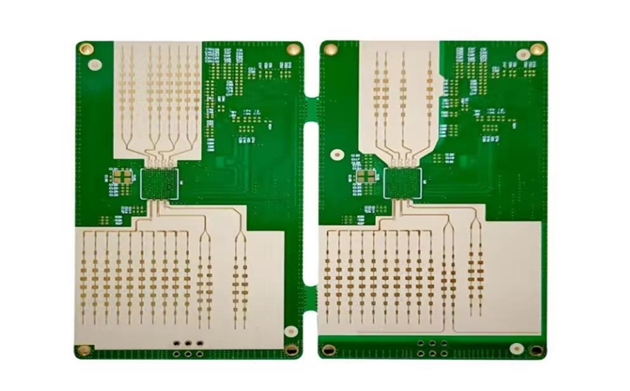
If you're new to printed circuit board (PCB) design, you might be wondering, "What is a PCB stackup, and why does it matter?" Simply put, a PCB stackup is the arrangement of copper and insulating layers that form a PCB. It’s a critical part of the design process because it impacts signal integrity, electromagnetic compatibility (EMC), and manufacturing costs. In this beginner's guide, we'll break down the basics of PCB stackups, including layer arrangement, materials, and key design rules, to help you create effective and reliable designs.
Whether you're just starting with PCB design or looking to understand the fundamentals of stackups, this tutorial will walk you through everything you need to know. Let’s dive into the world of PCB stackups and explore how they shape the performance of your electronic projects.
What Is a PCB Stackup? A Simple Explanation for Beginners
A PCB stackup refers to the way layers of conductive copper and insulating materials are arranged in a printed circuit board. Think of it as a sandwich: the copper layers are like the bread, carrying electrical signals, while the insulating layers (often called dielectric materials) are the filling, keeping the copper layers separate to prevent short circuits.
Stackups are essential because they determine how signals travel through the board, how much interference they encounter, and how well the board can handle high-speed data. A well-designed stackup can reduce noise, improve signal quality, and make your PCB more reliable. On the other hand, a poorly planned stackup can lead to issues like crosstalk, electromagnetic interference (EMI), and even complete circuit failure.
For beginners, understanding stackups starts with recognizing that most PCBs aren’t just a single layer. Many modern designs use multiple layers—sometimes 4, 6, 8, or more—to fit complex circuits into a small space. The arrangement of these layers is what we call the stackup.
Why PCB Stackups Matter in Design
The stackup isn’t just about stacking layers randomly; it’s a deliberate design choice that affects several aspects of your PCB’s performance:
- Signal Integrity: High-speed signals, such as those in USB or HDMI circuits, need a consistent path to avoid distortion. A proper stackup ensures signals travel without interference.
- Electromagnetic Compatibility (EMC): A good stackup minimizes EMI, preventing your board from interfering with other devices or being affected by external noise.
- Impedance Control: For high-speed designs, maintaining a specific impedance (often 50 ohms for RF signals) is crucial. The stackup directly impacts this value.
- Cost and Manufacturability: More layers mean higher costs. A well-planned stackup balances performance with budget constraints.
For example, in a 4-layer PCB, a common stackup might dedicate the top and bottom layers to signals, while the inner layers serve as ground and power planes. This setup helps shield signals from interference and provides a stable reference for impedance, ensuring better performance for high-speed circuits.
Understanding PCB Layers: Breaking Down the Structure
Let’s take a closer look at the different types of layers in a PCB stackup. Most PCBs are made up of two primary components: copper layers and dielectric layers. Here's what each does:
Copper Layers: The Conductive Pathways
Copper layers are where the electrical signals flow. These layers are etched to create traces, pads, and other conductive paths that connect components. In a multi-layer PCB, copper layers are categorized based on their purpose:
- Signal Layers: Used for routing signals between components. These are often on the outer layers (top and bottom) for easy access during assembly.
- Power and Ground Planes: These are solid copper layers dedicated to providing stable power or a common ground reference. They help reduce noise and are usually placed in the inner layers.
Dielectric Layers: The Insulators
Dielectric layers are made of insulating materials that separate the copper layers. They prevent short circuits and play a key role in determining the board’s electrical properties, such as impedance. The thickness and material of these layers are critical in high-speed designs.
For instance, in a 4-layer PCB, a typical stackup might look like this:
- Top Layer (Signal)
- Dielectric Layer
- Inner Layer 1 (Ground Plane)
- Dielectric Layer
- Inner Layer 2 (Power Plane)
- Dielectric Layer
- Bottom Layer (Signal)
This arrangement ensures that signal layers are close to reference planes (ground or power), which helps maintain signal integrity by providing a consistent return path for currents.
Common PCB Stackup Configurations for Beginners
PCB stackups come in various configurations depending on the complexity of the design. Here are the most common setups for beginners to understand:
2-Layer Stackup
A 2-layer PCB is the simplest multi-layer design, often used in basic projects. It consists of a top and bottom copper layer separated by a dielectric material. This stackup is ideal for low-cost, low-complexity circuits but offers limited space for routing and poor noise control.
4-Layer Stackup
A 4-layer PCB is a popular choice for many hobbyists and professionals because it balances cost and performance. As mentioned earlier, it typically has two signal layers on the outside and two inner planes (ground and power). This setup improves signal integrity and EMC compared to a 2-layer board.
6-Layer and Beyond
For more complex designs, such as those in smartphones or high-speed communication devices, 6-layer or higher stackups are used. These allow for more signal layers and additional planes to manage noise and impedance. A common 6-layer stackup might include:
- Top Signal Layer
- Ground Plane
- Signal Layer
- Power Plane
- Signal Layer
- Bottom Signal Layer
As the number of layers increases, so does the complexity of routing and manufacturing costs. For beginners, starting with a 4-layer design is often a good middle ground.
Materials Used in PCB Stackups: What You Need to Know
The materials in a PCB stackup play a huge role in its performance, especially for high-frequency or high-speed applications. Here are the key materials involved:
Dielectric Materials
The dielectric material is the insulator between copper layers. The most common material is FR-4, a fiberglass-reinforced epoxy laminate. FR-4 is widely used due to its low cost and decent electrical properties. It has a dielectric constant (Dk) of around 4.2 to 4.5, which affects signal speed and impedance.
For high-frequency designs, materials like Rogers or Isola are used because they have lower Dk values (around 3.0 to 3.5) and better signal performance. However, these materials are more expensive and may not be necessary for beginner projects.
Copper Foil
The copper layers are typically made from rolled or electrodeposited copper foil. The thickness of the copper, measured in ounces per square foot (oz/ft2), affects the current-carrying capacity. Common thicknesses are 1 oz/ft2 (about 35 micrometers) for standard designs and 2 oz/ft2 for higher current needs.
Prepreg and Core
In multi-layer PCBs, dielectric layers are made of two components: the core and prepreg. The core is a rigid, pre-cured layer, while prepreg is a partially cured material that bonds the layers together during manufacturing. The thickness of these layers (often between 0.1 mm and 0.2 mm for inner layers) impacts the overall board thickness and impedance.
Key Design Rules for PCB Stackups
Designing a PCB stackup isn’t just about stacking layers; it involves following specific rules to ensure performance and manufacturability. Here are some essential design rules for beginners:
1. Keep Signal Layers Close to Reference Planes
Always place signal layers next to a ground or power plane. This minimizes the loop area for return currents, reducing noise and improving signal integrity. For example, in a 4-layer board, the top signal layer should be adjacent to a ground plane.
2. Control Layer Thickness for Impedance
Impedance matching is critical for high-speed signals. The dielectric thickness between a signal layer and its reference plane affects impedance. For a 50-ohm trace, a dielectric thickness of 0.1 mm with FR-4 material might be used. Use impedance calculators or consult with your manufacturer to get the right values.
3. Avoid Asymmetrical Stackups
An asymmetrical stackup (uneven layer distribution) can cause the board to warp during manufacturing. For example, in a 6-layer PCB, ensure that the layers are balanced, with similar thicknesses on both sides of the center.
4. Minimize Crosstalk with Proper Layer Spacing
Crosstalk occurs when signals on adjacent layers interfere with each other. Increase the dielectric thickness between signal layers or use ground planes to shield them. A spacing of at least 0.2 mm between signal layers can help reduce crosstalk in many designs.
5. Plan for Manufacturing Constraints
Check with your PCB fabricator for their capabilities, such as minimum dielectric thickness or maximum layer count. Designing within these limits prevents costly redesigns. For instance, standard FR-4 boards often have a total thickness of 1.6 mm, which is widely supported.
Tips for Beginners to Create an Effective PCB Stackup
Now that you understand the basics of PCB stackups, here are some practical tips to help you design your first board:
- Start Simple: Begin with a 2-layer or 4-layer design to learn the basics before moving to more complex stackups.
- Use Design Software: Tools with layer stack managers can help you visualize and configure your stackup. They often include impedance calculators for accurate planning.
- Consult Your Manufacturer Early: Share your stackup design with your fabricator to ensure it’s manufacturable and cost-effective.
- Focus on Ground Planes: A solid ground plane near signal layers is one of the easiest ways to improve signal quality.
- Learn from Examples: Study stackup configurations for common applications, like microcontrollers or RF circuits, to understand best practices.
Common Mistakes to Avoid in PCB Stackup Design
As a beginner, it’s easy to make mistakes when designing a PCB stackup. Here are some pitfalls to watch out for:
- Ignoring Impedance Needs: Failing to calculate impedance for high-speed signals can lead to signal distortion. Always verify dielectric thickness and trace width.
- Overcomplicating the Design: Adding unnecessary layers increases costs without improving performance. Stick to the minimum layers needed for your circuit.
- Poor Layer Arrangement: Placing signal layers far from ground planes increases noise. Follow the rule of keeping signals close to reference planes.
- Forgetting Thermal Management: High-power designs need thicker copper or additional planes for heat dissipation. Plan for this in your stackup.
Conclusion: Mastering PCB Stackups as a Beginner
Understanding PCB stackups is a fundamental skill for anyone stepping into the world of electronics design. By learning how to arrange layers, choose the right materials, and follow essential design rules, you can create boards that are reliable, efficient, and cost-effective. Start with simple designs, like a 4-layer stackup, and gradually build your skills as you tackle more complex projects.
Remember, a good stackup is the foundation of a successful PCB. It ensures your signals are clean, your board is free from interference, and your design can be manufactured without issues. With the tips and guidelines in this beginner’s guide, you’re well on your way to mastering PCB stackups and bringing your electronic ideas to life.
Keep experimenting, learning, and refining your approach to stackup design. The more you practice, the more intuitive it will become. Happy designing!
 ALLPCB


