 ALLPCB


When designing a printed circuit board (PCB), one critical decision is how to manage copper distribution. Two common techniques—copper balancing and copper pouring—play vital roles in ensuring performance, manufacturability, and reliability. So, which is right for your PCB? Copper balancing focuses on evenly distributing copper across layers to prevent warping and ensure consistent etching during manufacturing, while copper pouring fills empty spaces with copper to improve grounding, thermal management, and signal integrity. The choice depends on your design goals, such as high-speed signal performance or structural stability. In this blog, we’ll dive deep into both techniques, comparing their benefits, challenges, and ideal applications to help you make an informed decision for your next project.
Understanding Copper in PCB Design
Copper is the backbone of any PCB, serving as the conductive material that carries electrical signals and power between components. However, how copper is distributed on a board significantly impacts its performance and manufacturing quality. Uneven copper can lead to issues like board warping, inconsistent etching, or signal interference. This is where techniques like copper balancing and copper pouring come into play. Both aim to optimize copper distribution but serve different purposes depending on the design needs. Let’s explore each method in detail to understand their roles in PCB design and manufacturing.
What Is Copper Balancing in PCB Design?
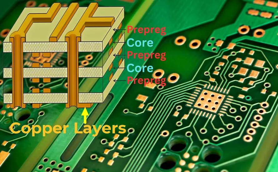
Copper balancing refers to the practice of evenly distributing copper across all layers of a PCB to maintain structural integrity and ensure uniform manufacturing processes. During PCB fabrication, processes like etching (removing unwanted copper) and plating (adding copper to vias and pads) rely on consistent copper density. If one area of the board has significantly more or less copper than another, it can lead to uneven etching rates, causing defects or weak traces. Additionally, imbalanced copper can create thermal stress during soldering, resulting in board warping—a serious issue that can render a PCB unusable.
To achieve copper balancing, designers often use techniques like adding dummy copper patterns or "thieving" in areas with low copper density. Thieving involves placing small, non-functional copper shapes in empty spaces to match the copper density of busier areas. This technique helps maintain uniformity without interfering with the board’s electrical performance. For example, if a PCB layer has a dense area with traces and pads on one side but is mostly empty on the other, adding thieving patterns can bring the copper density to around 50-60% across the board, reducing manufacturing risks.
Key Benefits of Copper Balancing:
- Prevents Warping: Balanced copper minimizes thermal stress during reflow soldering, keeping the board flat.
- Improves Manufacturing Consistency: Uniform copper distribution ensures even etching and plating, reducing defects.
- Enhances Durability: A structurally stable PCB is less likely to crack or deform over time.
Challenges of Copper Balancing:
- Design Complexity: Adding dummy copper or adjusting layouts requires extra time and attention to detail.
- Limited Electrical Impact: Unlike copper pouring, balancing doesn’t directly improve grounding or signal performance.
Copper balancing is especially critical in multilayer PCBs, where uneven copper across layers can amplify warping risks. It’s a must for designs prioritizing mechanical stability over electrical enhancements.
What Is Copper Pouring in PCB Design?
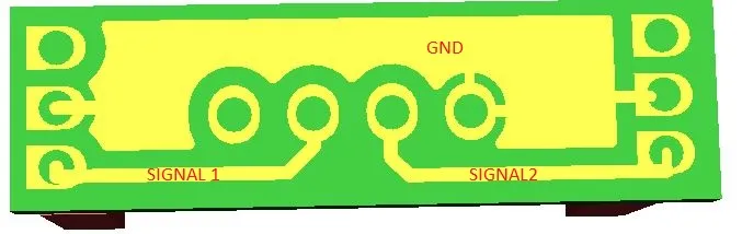
Copper pouring, also known as copper fill or copper flooding, involves filling unused areas of a PCB layer with copper, typically connected to a specific net like ground or power. This technique is widely used to enhance electrical and thermal performance. By creating large copper areas, designers can provide a low-impedance return path for signals, reduce electromagnetic interference (EMI), and improve heat dissipation from components. Copper pours are often applied on ground planes or signal layers where space allows.
For instance, in high-speed designs operating at frequencies above 100 MHz, a solid copper pour connected to ground can significantly reduce noise and crosstalk between traces. It acts as a shield, minimizing EMI that could disrupt signal integrity. Additionally, copper pours help manage heat in power-intensive designs by spreading thermal energy away from hot components, potentially reducing the junction temperature of a power IC by 10-15°C in some cases.
Key Benefits of Copper Pouring:
- Improved Signal Integrity: A ground-connected pour reduces noise and provides a stable reference plane for high-speed signals.
- Thermal Management: Copper acts as a heat sink, dissipating heat from components to prevent overheating.
- EMI Reduction: Large copper areas shield sensitive circuits from external or internal interference.
- Manufacturing Support: Copper pours can help balance copper to some extent, aiding etching uniformity.
Challenges of Copper Pouring:
- Parasitic Capacitance: Too much copper near high-frequency traces can introduce unwanted capacitance, affecting signal timing.
- Thermal Relief Issues: Without proper thermal relief pads, soldering components directly on large copper areas can result in cold joints.
- Floating Copper Risk: Unconnected copper pours can act as antennas, picking up or emitting EMI and causing interference.
Copper pouring shines in designs where electrical performance, such as grounding or heat dissipation, takes precedence over pure structural concerns. It’s a go-to choice for high-speed and high-power applications.
Comparing Copper Balancing and Copper Pouring: Key Differences
While both copper balancing and copper pouring involve managing copper distribution on a PCB, their purposes and outcomes differ significantly. Understanding these differences is crucial for selecting the right approach for your design. Let’s break it down:
1. Primary Purpose:
- Copper Balancing: Focuses on structural stability and manufacturing consistency by ensuring even copper density across layers.
- Copper Pouring: Aims to enhance electrical performance, thermal management, and EMI shielding by filling empty spaces with functional copper.
2. Electrical Impact:
- Copper Balancing: Has minimal direct impact on electrical performance since dummy copper or thieving is often non-functional.
- Copper Pouring: Directly improves grounding, reduces impedance (often to below 50 ohms for high-speed signals), and minimizes noise.
3. Manufacturing Considerations:
- Copper Balancing: Primarily addresses etching and plating uniformity, reducing defects by maintaining a copper density of 40-60% across the board.
- Copper Pouring: Can aid manufacturing by balancing copper but risks uneven distribution if not applied symmetrically across layers.
4. Design Complexity:
- Copper Balancing: Requires careful planning to place dummy copper without interfering with functional areas, adding time to the layout process.
- Copper Pouring: Needs attention to net connections (ground or power) and clearance rules to avoid parasitic effects or soldering issues.
In short, copper balancing is ideal for preventing physical issues like warping, while copper pouring excels in boosting electrical and thermal performance. Often, the two techniques can complement each other in a single design.
When to Use Copper Balancing in PCB Manufacturing
Copper balancing is the right choice when your primary concern is the structural integrity and manufacturability of your PCB. Here are some specific scenarios where it’s most effective:
- Multilayer PCBs: With multiple layers, uneven copper distribution can cause significant warping. Balancing ensures each layer has a similar copper density (ideally within 10-15% of each other).
- Large Boards: Larger PCBs are more prone to bending or twisting during manufacturing. Copper balancing helps maintain flatness.
- High-Volume Production: In mass production, consistent etching and plating are critical to avoid defects. Balancing copper reduces variability in the fabrication process.
- Designs with Uneven Trace Density: If one area of your board has dense routing and another is mostly empty, thieving or dummy copper can prevent manufacturing issues.
For example, in a 6-layer PCB for an industrial control system, where signal speed isn’t a primary concern but reliability is, copper balancing across layers can prevent mechanical failures during assembly or operation.
When to Use Copper Pouring in PCB Manufacturing
Copper pouring is the better option when electrical performance and thermal management are top priorities. Consider using it in these situations:
- High-Speed Designs: For circuits operating at frequencies above 50 MHz, a ground-connected copper pour reduces noise and ensures a low-impedance return path (often below 1 ohm).
- Power Electronics: In designs with high current or heat-generating components, copper pours spread thermal energy, keeping component temperatures within safe limits (e.g., below 85°C for most ICs).
- EMI-Sensitive Applications: Copper pours connected to ground can shield sensitive analog or RF circuits from interference, reducing noise by up to 20 dB in some cases.
- Compact Designs: In densely packed boards, copper pours on inner layers can provide additional grounding without requiring extra space.
For instance, in a PCB for a wireless communication device operating at 2.4 GHz, a solid copper pour on the ground plane can minimize signal crosstalk and ensure reliable performance.
Can You Combine Copper Balancing and Copper Pouring?
Absolutely! In many cases, combining both techniques yields the best results. Copper pouring can contribute to balancing by filling empty spaces, while thieving or dummy copper can fine-tune density in areas where pours aren’t feasible or connected to a net. For example, in a 4-layer PCB, you might use copper pours on the inner ground and power planes for electrical benefits, then add thieving patterns on signal layers to achieve uniform density without affecting performance.
The key is symmetry. Ensure that copper distribution remains consistent across layers to avoid warping, and always connect pours to appropriate nets (like ground) to prevent floating copper issues. Design software tools often include features to check copper density and suggest balancing patterns, making it easier to integrate both methods.
Best Practices for Copper Management in PCB Design
Whether you choose copper balancing, copper pouring, or a combination of both, following these best practices will help optimize your PCB design:
- Check Copper Density: Aim for a copper density of 40-60% across each layer to ensure manufacturing consistency.
- Use Thermal Reliefs: For copper pours, add thermal relief pads around through-hole components to prevent soldering issues.
- Avoid Floating Copper: Always connect copper pours to a net (usually ground) to prevent them from acting as antennas for EMI.
- Maintain Clearance Rules: Keep sufficient spacing between copper pours and traces (e.g., 0.2 mm or more) to avoid parasitic capacitance or shorts.
- Symmetrical Layer Stackup: Design your layer stackup with balanced copper distribution to minimize thermal stress and warping.
- Simulate and Test: Use design tools to simulate signal integrity and thermal performance, especially for high-speed or high-power designs with copper pours.
By adhering to these guidelines, you can maximize the benefits of copper management while minimizing potential drawbacks.
Conclusion: Making the Right Choice for Your PCB
Choosing between copper balancing and copper pouring—or deciding to use both—depends on the specific needs of your PCB design. If your focus is on structural stability and manufacturing reliability, copper balancing with thieving patterns is essential to prevent warping and ensure consistent fabrication. On the other hand, if signal integrity, thermal management, or EMI reduction are your priorities, copper pouring offers significant electrical and thermal advantages. For many modern designs, a hybrid approach provides the best of both worlds, combining the mechanical benefits of balancing with the performance boosts of pouring.
Ultimately, understanding your project’s requirements—whether it’s a high-speed communication board or a robust industrial controller—will guide your decision. With careful planning and adherence to design best practices, you can achieve a PCB that performs reliably and is easy to manufacture. At ALLPCB, we’re committed to supporting your design journey with high-quality manufacturing solutions tailored to your copper management needs. Let’s build better boards together.


