 ALLPCB


If you're dealing with a malfunctioning mobile phone, the Printed Circuit Board (PCB) is often at the heart of the problem. Whether it's a short circuit, broken trace, or a faulty component, knowing how to troubleshoot and repair a mobile phone PCB can save you time and money. In this comprehensive guide, we'll walk you through the most common issues with mobile phone PCBs and provide step-by-step solutions for PCB short circuit repair, broken trace repair, component replacement on PCB, multimeter testing for PCB, and using a PCB rework station. Let's dive into the details to help you get your device back in working order.
Understanding the Mobile Phone PCB: The Heart of Your Device
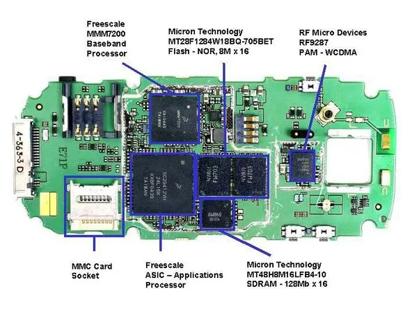
A mobile phone PCB is a complex board that connects all the electronic components of the device, such as the processor, memory, and power management circuits. It acts as the central hub, ensuring that signals and power flow correctly between components. When something goes wrong with the PCB, the phone may fail to power on, lose signal, or exhibit other performance issues.
Common problems with mobile phone PCBs include short circuits, damaged traces, and failed components. These issues can stem from physical damage, water exposure, or manufacturing defects. By learning to identify and fix these problems, you can extend the life of your device. Before we get into specific repair techniques, let's look at the tools you'll need for effective troubleshooting and repair.
Essential Tools for Mobile Phone PCB Repair
Repairing a mobile phone PCB requires precision and the right equipment. Here's a list of essential tools to have on hand:
- Multimeter: Used for multimeter testing on PCB to check voltage, continuity, and resistance. This helps identify short circuits and open traces.
- Soldering Iron or PCB Rework Station: A PCB rework station is ideal for desoldering and soldering components with precision, especially for surface-mount devices (SMDs).
- Magnifying Glass or Microscope: Essential for inspecting tiny traces and solder joints on the PCB.
- Tweezers and Screwdrivers: For handling small components and disassembling the phone.
- Isopropyl Alcohol and Brush: For cleaning the PCB after repairs to remove flux residue or contaminants.
- Replacement Components: Keep spare capacitors, resistors, and ICs that are commonly found on mobile phone PCBs.
With these tools ready, you're equipped to tackle most PCB issues. Now, let's explore the common problems and how to fix them.
Common Mobile Phone PCB Issues and How to Troubleshoot Them
Mobile phone PCBs can fail for various reasons, but some issues are more common than others. Below, we'll cover the most frequent problems and provide actionable solutions.
1. PCB Short Circuit Repair: Identifying and Fixing Shorts
A short circuit occurs when two points on the PCB that shouldn't be connected come into contact, often due to water damage, solder bridges, or component failure. This can cause the phone to overheat, fail to turn on, or drain the battery quickly.
Steps for PCB Short Circuit Repair:
- Visual Inspection: Start by examining the PCB under a magnifying glass. Look for signs of burnt areas, solder splashes, or corrosion, especially around power lines.
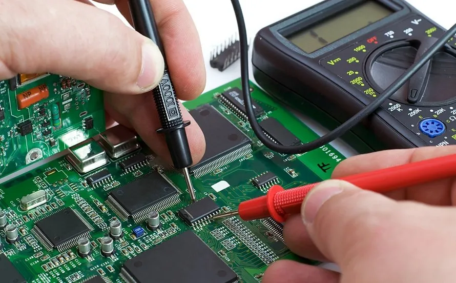
- Multimeter Testing for PCB: Set your multimeter to continuity mode. Test between the power line (VCC) and ground (GND) to check for a short. If the multimeter beeps or shows a low resistance value (e.g., below 10 ohms), there's likely a short circuit.
- Isolate the Short: Use the multimeter to trace the short by testing individual components or sections of the PCB. Common culprits include capacitors or diodes near the power management IC.
- Remove the Faulty Component: If a component is causing the short, use a PCB rework station to desolder it carefully. Replace it with a new component if necessary.
- Clean and Test: After repair, clean the area with isopropyl alcohol and retest with the multimeter to ensure the short is resolved.
2. Broken Trace Repair: Restoring Connectivity
Traces are the tiny copper pathways on a PCB that connect components. A broken trace repair is needed when these pathways are damaged due to physical stress, corrosion, or overheating. A broken trace can result in loss of functionality, such as a non-working button or charging port.
Steps for Broken Trace Repair:
- Locate the Break: Use a magnifying glass to find the damaged trace. Look for visible cracks or areas where the copper has lifted off the board.
- Clean the Area: Gently scrape away any debris or corrosion around the broken trace using a fine tool or brush. Clean with isopropyl alcohol.
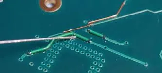
- Bridge the Gap: For small breaks, apply a thin layer of conductive paint or solder a small jumper wire to reconnect the trace. For larger breaks, you may need to solder a thin copper wire across the gap.
- Secure the Repair: Once the connection is made, cover the repaired area with a small amount of insulating tape or UV-curable mask to prevent future shorts.
- Test Continuity: Use your multimeter in continuity mode to confirm that the trace is now conducting properly.
Repairing traces requires a steady hand and patience, but it can restore full functionality to the PCB.
3. Component Replacement on PCB: Swapping Out Faulty Parts
Components like capacitors, resistors, and ICs on a mobile phone PCB can fail over time due to heat, voltage spikes, or physical damage. Component replacement on PCB is a common repair task that can fix issues like power failure or audio problems.
Steps for Component Replacement on PCB:
- Identify the Faulty Component: Use schematics or reference designs for the specific phone model to pinpoint the problematic part. Test components with a multimeter if possible. For example, a capacitor showing no capacitance (reading 0 farads) is likely faulty.
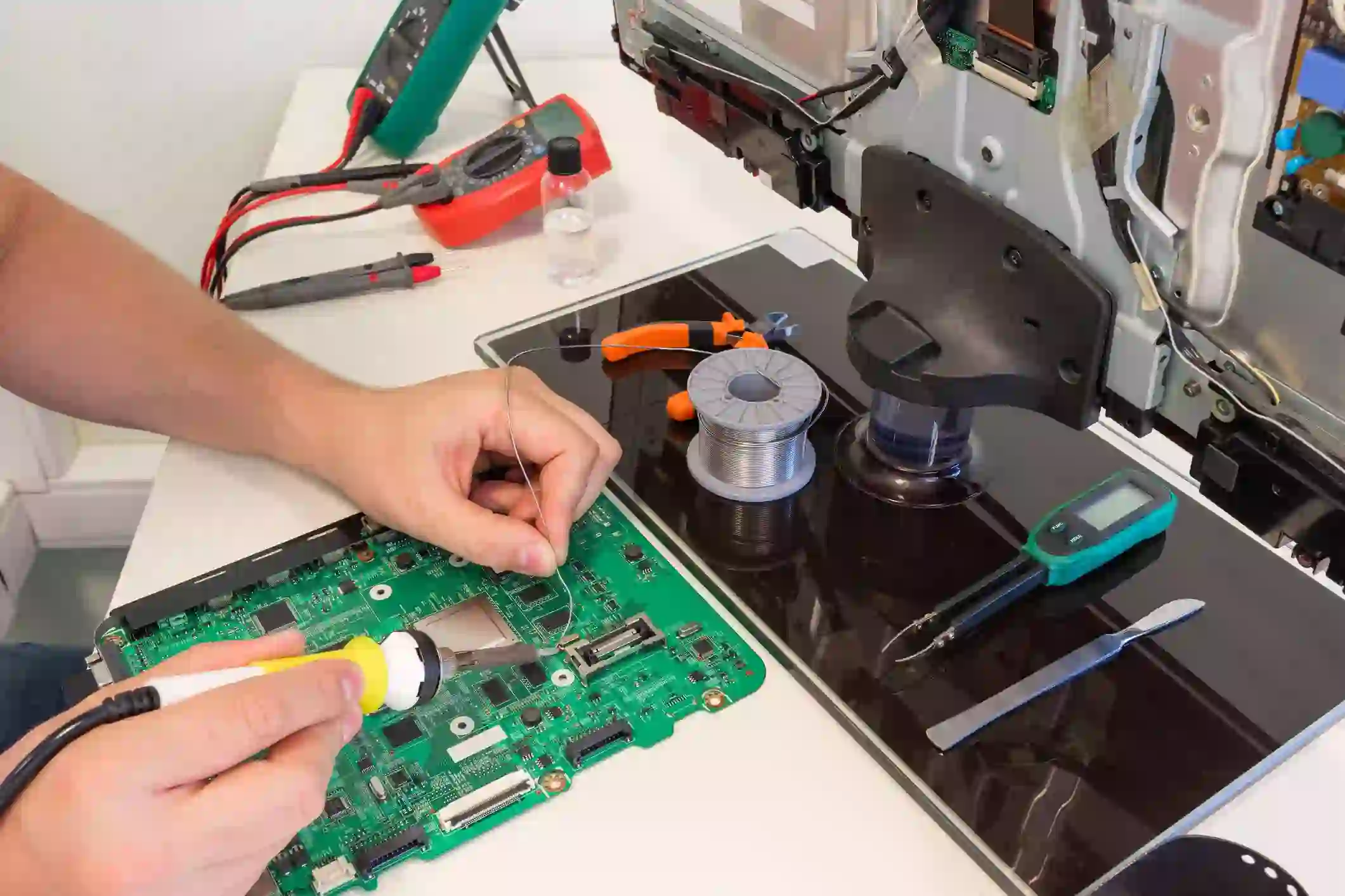
- Desolder the Component: Use a PCB rework station with hot air to carefully remove the faulty component. Heat the solder joints evenly (around 300°C for most SMD parts) and lift the component with tweezers.
- Clean the Pads: Remove old solder from the pads using a soldering iron and wick. Clean the area with isopropyl alcohol.
- Install the New Component: Place the replacement component on the pads, aligning it correctly. Apply fresh solder or use hot air to secure it in place.
- Test the Repair: Power on the device or use a multimeter to verify that the new component is functioning. For instance, a replaced capacitor should show a capacitance value within the expected range (e.g., 10 μF if specified).
Precision is key when replacing components, as overheating or misalignment can cause further damage.
4. Multimeter Testing for PCB: Diagnosing Electrical Issues
Multimeter testing for PCB is a fundamental skill for diagnosing issues like short circuits, open circuits, and component failures. A multimeter can measure voltage, resistance, and continuity, providing insight into the health of the PCB.
How to Perform Multimeter Testing for PCB:
- Power Off the Device: Always disconnect the battery or power source before testing to avoid damage or injury.
- Check Voltage: Set the multimeter to DC voltage mode and test key points like the battery connector or power IC output. For most mobile phones, the battery voltage should read between 3.7V and 4.2V when fully charged.
- Test Continuity: Switch to continuity mode to check for broken traces or connections. A beep indicates a complete circuit, while silence means an open circuit.
- Measure Resistance: Use resistance mode to test components like resistors. Compare the measured value (e.g., 1 kΩ) to the expected value marked on the component or schematic.
- Identify Shorts: As mentioned earlier, test between power and ground lines to detect shorts with low resistance readings.
Regular multimeter testing can help you narrow down issues quickly and accurately.
5. Using a PCB Rework Station for Precision Repairs
A PCB rework station is an advanced tool that combines hot air and soldering capabilities, making it ideal for working on small, delicate components found in mobile phone PCBs. It’s especially useful for tasks like desoldering SMD components or reballing ICs.
Benefits of Using a PCB Rework Station:
- Precision Heating: Hot air can be directed to specific areas, preventing damage to nearby components. Typical temperatures range from 250°C to 350°C for most repairs.
- Versatility: Many rework stations come with interchangeable nozzles for different component sizes, from tiny capacitors to larger ICs.
- Efficiency: Rework stations speed up the process of desoldering and soldering compared to traditional soldering irons.
Tips for Using a PCB Rework Station:
- Always start with a lower temperature and increase as needed to avoid overheating the PCB.
- Use heat-resistant tape to protect nearby components from hot air.
- Practice on scrap boards to get a feel for the tool before working on a valuable device.
Investing in a good rework station can significantly improve the quality of your repairs.
Preventing Future PCB Issues
While knowing how to repair a mobile phone PCB is valuable, preventing damage in the first place is even better. Here are some tips to protect your device’s PCB:
- Use a Protective Case: A sturdy case can prevent physical damage to the phone, which often leads to PCB issues.
- Avoid Water Exposure: Keep your phone away from liquids, as moisture can cause corrosion and short circuits on the PCB.
- Handle with Care During Repairs: Use an anti-static wrist strap to prevent static discharge, which can damage sensitive components.
- Regular Maintenance: If you frequently repair phones, clean the PCB periodically with isopropyl alcohol to remove dust and debris.
Conclusion: Mastering Mobile Phone PCB Repair
Repairing a mobile phone PCB can seem daunting at first, but with the right tools and techniques, it’s a skill you can develop. Whether you’re tackling PCB short circuit repair, performing broken trace repair, doing component replacement on PCB, using multimeter testing for PCB, or working with a PCB rework station, each step brings you closer to restoring your device. By following the detailed steps in this guide, you can troubleshoot common issues and bring your mobile phone back to life.
Remember to take your time, work methodically, and prioritize safety when handling electronic components. With practice, you’ll gain confidence in handling even the most complex PCB repairs. Stay equipped, stay precise, and keep your devices running smoothly!





