 ALLPCB


Introduction
Wearable IoT devices continue to expand in applications ranging from health monitoring to industrial sensing. These compact systems rely heavily on flexible printed circuit boards to conform to curved surfaces and moving body parts. Designers increasingly focus on sustainability to address growing concerns over electronic waste and resource consumption. Low power flex PCB for iot implementations help extend battery life while reducing overall energy demands during operation. Energy harvesting wearable flex pcb approaches further minimize reliance on traditional power sources by capturing ambient energy. Material choices that support biodegradable flex pcb for iot or recyclable flex pcb design contribute to lower environmental impact wearable pcb outcomes across the product lifecycle.
Why Sustainable Flex PCB Design Matters
Flexible circuits in wearables must balance mechanical flexibility, electrical performance, and long-term reliability under repeated bending and environmental exposure. Sustainable design practices address these requirements while aligning with broader industry goals for reduced material use and improved end-of-life management. Engineers evaluate substrate materials, conductor layouts, and component integration to limit power draw without compromising signal integrity. Recyclable flex pcb design strategies emphasize separable layers and compatible material combinations that facilitate disassembly and recovery. Environmental impact wearable pcb assessments consider factors such as raw material sourcing, manufacturing energy, and disposal pathways. These considerations support compliance with evolving regulatory expectations for electronics producers.
Technical Principles of Low-Power and Energy-Efficient Flex PCB Architectures
Low power flex PCB for iot designs begin with careful selection of trace widths, via structures, and dielectric thicknesses that minimize resistive losses and parasitic capacitance. Engineers apply simulation tools to model current distribution and thermal behavior under dynamic flexing conditions. Energy harvesting wearable flex pcb systems integrate transducers such as piezoelectric films or photovoltaic elements directly onto the flexible substrate. These elements convert mechanical motion or light into usable electrical energy that supplements or replaces battery power. Substrate materials must maintain stable electrical properties across temperature and humidity ranges typical of wearable use. Power management circuitry, including efficient voltage regulators and sleep-mode protocols, further reduces average consumption during intermittent data transmission cycles.
Material Considerations for Recyclable and Biodegradable Flex Circuits
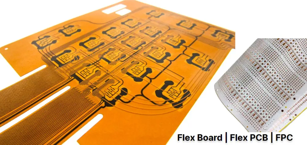
Traditional polyimide substrates offer excellent thermal stability and flexibility but present challenges for recycling due to their chemical structure. Alternative polymer systems under evaluation include certain polyester and bio-based films that support biodegradable flex pcb for iot pathways when combined with appropriate conductor materials. Conductive inks and adhesives formulated for easier separation during recycling processes help achieve recyclable flex pcb design targets. Layer stack-ups are optimized to avoid permanent bonding between dissimilar materials that would hinder mechanical or chemical recovery methods. Testing protocols evaluate flexural endurance alongside environmental degradation rates under controlled conditions. These material decisions directly influence both device performance and end-of-life environmental impact wearable pcb metrics.
Related Reading: Unlocking Sustainability: The Science Behind Biodegradable PCB Substrates
Best Practices for Sustainable Design Implementation
Design teams begin by defining power budgets early in the project and mapping energy requirements against available harvesting sources. Component placement prioritizes low-quiescent-current devices and minimizes interconnect lengths to reduce resistive losses. Ground planes and shielding layers are configured to maintain signal quality while avoiding unnecessary copper usage. Modular layouts that allow selective replacement of sections rather than entire assemblies extend product usability and reduce waste. Documentation of material composition supports downstream recycling streams and regulatory reporting. Collaboration between electrical, mechanical, and materials engineers ensures that flexibility requirements do not compromise power efficiency or recyclability goals.
Environmental Impact Assessment in Wearable PCB Development
Quantifying environmental impact wearable pcb involves life-cycle thinking that spans raw material extraction through manufacturing, use, and disposal phases. Metrics include cumulative energy demand, greenhouse gas emissions, and potential for material recovery. Low power flex PCB for iot architectures reduce operational energy consumption, which often dominates the use-phase footprint in battery-powered devices. Energy harvesting wearable flex pcb features further lower this contribution by decreasing battery replacement frequency. At end of life, designs incorporating recyclable flex pcb design principles enable higher recovery rates of metals and polymers. Biodegradable flex pcb for iot options are considered where controlled composting or degradation environments exist, though performance validation remains essential.
Related Reading: The Environmental Impact of Improper PCB Disposal: Why Recycling Matters
Conclusion
Sustainable flex PCB design integrates low-power techniques, energy harvesting, and material strategies to meet the performance needs of wearable IoT devices while addressing environmental considerations. Structured engineering approaches, grounded in established qualification methods, enable reliable operation under flexing and environmental stresses. Material and layout decisions that support recyclability or biodegradability contribute to reduced overall impact without sacrificing functionality. Continued refinement of these practices supports both technical requirements and broader sustainability objectives in electronics design.
FAQs
Q1: What defines a low power flex PCB for iot applications?
A1: A low power flex PCB for iot prioritizes reduced current draw through optimized trace geometry, efficient power management components, and substrate materials with low dielectric losses. These designs extend operating time between charges or harvests while maintaining reliable wireless connectivity and sensor performance in wearable form factors. Engineers validate performance through bench testing and simulation across expected flex cycles and temperature ranges.
Q2: How does energy harvesting integrate into wearable flex pcb designs?
A2: Energy harvesting wearable flex pcb incorporates thin-film transducers that convert body motion, light, or thermal gradients into electrical energy. The harvested power conditions and stores in small capacitors or batteries to supplement primary sources. Layout considerations ensure mechanical compatibility with the flexible substrate and minimal interference with primary circuit functions.
Q3: What approaches support biodegradable flex pcb for iot development?
A3: Biodegradable flex pcb for iot explores polymer substrates and conductors designed to break down under specific environmental conditions after the device reaches end of life. Material selection balances initial electrical and mechanical properties with controlled degradation rates. Validation includes both functional testing and standardized degradation studies to confirm suitability for target applications.
Q4: How can recyclable flex pcb design reduce environmental impact wearable pcb outcomes?
A4: Recyclable flex pcb design uses separable layers, compatible adhesives, and documented material compositions that facilitate disassembly and material recovery. These practices lower the environmental impact wearable pcb by increasing the fraction of metals and polymers reclaimed rather than landfilled. Design documentation supports compliance with recycling standards and improves overall resource efficiency.





