 ALLPCB


Solder mask bridges, also called solder mask dams, play a critical role in modern printed circuit board manufacturing. These features consist of narrow strips of solder mask material positioned between closely spaced copper pads. Their primary function is to create a physical barrier that stops molten solder from flowing across gaps during the reflow process. In designs that incorporate fine-pitch components such as ball grid arrays and quad flat packages, uncontrolled solder movement can easily produce electrical shorts. Proper dam implementation therefore supports both assembly yield and long-term board reliability.
What Is a Solder Mask Bridge (Dam) and Why It Matters
A solder mask bridge is a defined section of solder mask that remains between adjacent pads after the mask is applied and cured. The dam width is typically specified during the PCB design phase and must account for manufacturing tolerances. Without these barriers, solder paste deposited on one pad can spread under the influence of surface tension and capillary action, forming an unintended connection to the neighboring pad. This phenomenon, known as solder bridging, becomes more probable as pad spacing decreases below 0.5 mm. The presence of dams helps maintain electrical isolation while still allowing sufficient solder volume for reliable joints.
Industry standards recognize the importance of controlled solder mask features for high-density interconnects. Designs that follow established guidelines reduce the risk of assembly defects and improve overall product quality.
Technical Principles and Mechanisms of Solder Bridging
Solder bridging arises from a combination of factors during surface-mount assembly. Excessive solder paste volume, insufficient pad spacing, and component placement inaccuracies all contribute to the problem. During reflow, the solder reaches its liquidus temperature and flows according to surface tension forces. When two pads are too close and no barrier exists, the molten alloy can form a continuous fillet that spans the gap.
A solder mask dam interrupts this flow by providing a raised or flush physical obstacle. The dam material, usually a liquid photoimageable solder mask, adheres to the board surface and withstands the thermal profile of reflow. Its height and width must be sufficient to contain the solder yet not so large that they interfere with paste deposition or component seating. In fine-pitch layouts, the dam also influences the final solder fillet shape, which affects joint strength and inspection criteria.
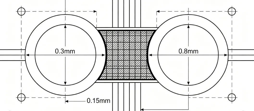
Thermal expansion differences between the mask, copper, and substrate can affect dam integrity. Proper material selection and curing parameters minimize cracking or delamination that might compromise the barrier function.
Practical Design and Manufacturing Best Practices
Effective solder mask dam design begins with clear spacing rules tailored to the component pitch and assembly process. Designers typically define minimum dam widths based on the solder mask resolution capability of the fabrication shop. Alignment between the mask artwork and the copper layer must remain within tight tolerances to avoid partial coverage of pads or encroachment into the dam area.
For ball grid array packages, dams are often placed in the spaces between perimeter pads or under the body where escape routing is dense. Quad flat package leads benefit from dams located between gull-wing or J-lead footprints to prevent bridging along the row. In both cases, the dam height should be considered relative to the stencil thickness so that paste release remains consistent.

Process controls during solder mask application further support dam performance. Accurate exposure and development ensure sharp dam edges and consistent thickness. Post-cure inspection verifies that no mask residue remains on pads and that dams are free of voids or thinning.
When changes occur in paste volume or reflow profile, engineers evaluate whether existing dam dimensions continue to provide adequate separation. Documentation of these parameters within the fabrication and assembly drawings helps maintain consistency across production runs.
Troubleshooting Common Solder Bridge Issues Related to Mask Design
Solder bridges that persist despite the presence of dams often trace back to mask misalignment or insufficient dam width. In such cases, review of the artwork files reveals whether the dam artwork overlaps copper or falls short of the intended gap. Increasing dam width within the limits of mask resolution frequently resolves the issue without altering pad geometry.
Another frequent cause involves mask thickness variations that allow solder to flow over the dam crest. Adjusting the mask formulation or application method can restore the barrier height. Engineers also examine stencil aperture design, because oversized apertures can deposit excess paste that overwhelms the dam capacity.

Systematic root-cause analysis that includes both design files and process data leads to targeted corrections rather than broad layout changes.
Conclusion
Solder mask bridges provide a reliable method for preventing solder bridging in fine-pitch PCB assemblies. Their effectiveness depends on accurate definition of width, alignment, and material properties during the design phase. When combined with appropriate assembly process controls, dams support high yields and robust electrical performance in complex boards containing ball grid arrays and quad flat packages. Attention to these details during layout and fabrication contributes directly to overall product quality.
FAQs
Q1: What is the purpose of a solder mask bridge in PCB design?
A1: A solder mask bridge, or dam, creates a physical barrier between adjacent pads to stop molten solder from forming unintended connections during reflow. This feature is especially important for fine-pitch components such as BGAs and QFPs where pad spacing is minimal. Proper dam implementation reduces the occurrence of solder bridging and supports reliable assembly.
Q2: How does solder mask dam width affect solder bridging prevention?
A2: Dam width determines the physical separation that molten solder must overcome. Narrower dams may be adequate for moderate pitches, while finer designs require wider dams within the resolution limits of the solder mask process. Consistent width across the board helps maintain uniform barrier performance.
Q3: Why are solder mask dams critical for BGA and QFP components?
A3: BGA and QFP packages place many leads or balls in close proximity, increasing the probability of solder flow between pads. Dams positioned between these terminations contain the solder volume and preserve electrical isolation. Their use aligns with accepted industry practices for high-density interconnect reliability.
Q4: What manufacturing factors influence solder mask dam effectiveness?
A4: Mask application accuracy, exposure settings, and curing conditions directly affect dam height, edge definition, and adhesion. Alignment between mask and copper layers must stay within specified tolerances. When these parameters are controlled, dams perform consistently across production batches.
References
IPC-A-600K — Acceptability of Printed Boards. IPC, 2020
IPC-6012E — Qualification and Performance Specification for Rigid Printed Boards. IPC, 2017
J-STD-001H — Requirements for Soldered Electrical and Electronic Assemblies. IPC, 2020





