 ALLPCB


Introduction
In RF PCB design, impedance matching ensures maximum power transfer and minimizes signal reflections, which is crucial for maintaining signal integrity at high frequencies. Engineers working on RF circuits face challenges from transmission line discontinuities that can degrade performance, leading to increased insertion loss and standing waves. This guide provides a structured overview of RF PCB impedance matching techniques, from calculation and measurement to implementing matching networks. By following established engineering principles, designers can achieve optimal signal transfer in applications like wireless communication and radar systems. Understanding these concepts allows for precise control over characteristic impedance, typically targeted at 50 ohms in RF systems. This tutorial equips electric engineers with practical steps to integrate impedance matching into their PCB layouts effectively.
What Is RF PCB Impedance Matching and Why It Matters
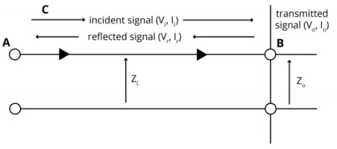
Impedance matching in RF PCBs refers to designing transmission lines and components so their characteristic impedance aligns with the source and load impedances. Characteristic impedance arises from the distributed inductance and capacitance along a transmission line, governed by geometry and substrate properties. Mismatches cause reflections, quantified by the reflection coefficient Γ = (Z_L - Z_0)/(Z_L + Z_0), where Z_L is load impedance and Z_0 is characteristic impedance. These reflections result in voltage standing wave ratio (VSWR) greater than 1, leading to power loss and signal distortion in RF signals.
The relevance intensifies at RF frequencies above 100 MHz, where wavelength approaches PCB trace lengths, turning them into transmission lines. Poor matching increases return loss, reduces antenna efficiency, and complies with performance specs in high-frequency designs. For electric engineers, mastering RF PCB impedance matching techniques prevents common pitfalls like crosstalk and EMI. Industry standards like IPC-2221 emphasize controlled impedance for reliable signal propagation. Ultimately, effective matching enhances overall system performance and yield during fabrication.
Technical Principles of Impedance in RF PCBs
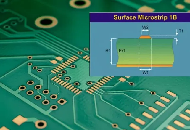
Transmission line theory forms the foundation, where characteristic impedance Z_0 = sqrt(L/C), with L as inductance per unit length and C as capacitance per unit length. In PCBs, microstrip lines expose one side to air, while striplines sandwich traces between ground planes, affecting field distribution and impedance. Dielectric constant (Er), trace width, thickness, and substrate height primarily determine Z_0. At RF frequencies, skin effect confines current to conductor surfaces, further influencing losses.
Frequency dependence introduces challenges, as effective Er varies, and dispersion alters phase velocity. Engineers must consider these for broadband matching. Common configurations include coplanar waveguides for easier integration with MMICs. Precise stack-up control ensures uniformity across the board. These principles guide RF PCB impedance calculation, enabling predictable behavior.
RF PCB Impedance Calculation Methods
Calculating impedance starts with selecting the transmission line type and gathering stack-up parameters like copper thickness, dielectric height, and Er. For microstrip, empirical equations approximate Z_0 based on width-to-height ratio and Er. IPC-2141A provides standardized formulas for high-speed controlled impedance, accounting for embedded traces and surface roughness. Software field solvers refine these for complex geometries, but initial estimates rely on closed-form expressions.
Factors like via stubs and bends introduce discontinuities, requiring de-embedding in calculations. Tolerance stacking from fab variations demands margins, typically ±10% for Z_0. Engineers iterate between layout and simulation during design. Substrate selection impacts Er stability over temperature and frequency. This systematic RF PCB impedance calculation ensures traces meet target Z_0 before prototyping.
RF PCB Impedance Measurement Techniques
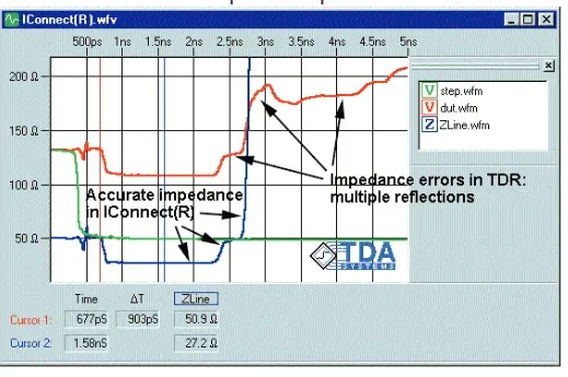
Post-fabrication verification uses time-domain reflectometry (TDR) to measure Z_0 along traces by analyzing step response reflections. TDR excels for detecting discontinuities like vias or impedance steps. Vector network analyzers (VNAs) provide frequency-domain S-parameters, from which Z_0 derives via TRL calibration. Test coupons on the PCB edge facilitate accurate measurements without desoldering components.
IPC-TM-650 outlines test methods for characteristic impedance using TDR, ensuring repeatability. De-embedding fixtures corrects for launch effects. Multi-line TRL methods enhance precision for differential pairs. Engineers compare measured Z_0 to design targets, adjusting future revisions. These RF PCB impedance measurement steps validate design assumptions and fab process control.
RF PCB Impedance Matching Techniques and Networks
When inherent Z_0 mismatches occur, matching networks transform impedances using lumped elements or distributed stubs. Series transmission line sections provide quarter-wave transformers for narrowband matching at f_0 where length = λ/4. Open or shorted stubs act as parallel resonators, tuning reactance.
L-networks, with one series and one shunt element, suit simple mismatches; pi-networks offer better bandwidth with two shunts and one series. For RF PCB impedance matching networks, select components with low parasitics, like chip capacitors rated for microwave frequencies. Layout minimizes parasitics by short paths and ground vias. Simulation optimizes values before implementation.
Best practices include symmetry in differential lines and avoiding meanders that alter Z_0. Ground plane stitching prevents slotline modes. This RF PCB impedance matching tutorial highlights iterative design: calculate, simulate, measure, and tweak. Multi-stage networks handle wideband requirements in modern 5G designs.
Troubleshooting Common Impedance Issues
Discontinuities from vias cause the most reflections; back-drilled or blind vias mitigate stubs. Uneven dielectric thickness from fab tolerances shifts Z_0; specify tight controls in fab notes. High Er variation with frequency demands low-loss materials. TDR reveals step changes, guiding fixes like trace widening.
Crosstalk arises from coupling; increase spacing or shielding. VSWR sweeps on VNA pinpoint issues. Post-layout extraction refines models. Case in point: a radar PCB showed 15 dB return loss after stub tuning, versus 5 dB initially. Systematic RF PCB impedance measurement and adjustment resolve these iteratively.
Conclusion
RF PCB impedance matching is essential for optimal signal transfer, blending theory, calculation, measurement, and practical networks. Engineers achieve this through precise stack-up design, standardized methods from IPC-2141A and IPC-TM-650, and verification tools. Implementing these techniques minimizes losses and ensures compliance in demanding RF applications. Regular iteration between design and test refines performance. By prioritizing controlled impedance, teams deliver robust, high-frequency PCBs ready for production.
FAQs
Q1: What are the key RF PCB impedance matching techniques for high-frequency designs?
A1: RF PCB impedance matching techniques include quarter-wave transformers, stub tuning, and lumped L, pi, or T networks. Select based on bandwidth needs: narrowband favors distributed elements, while wideband uses multi-stage lumped. Simulate reactance slopes and layout for minimal parasitics. Verify with TDR or VNA to confirm VSWR below 1.5. These methods ensure efficient power transfer in RF systems.
Q2: How do you perform RF PCB impedance calculation accurately?
A2: Start with stack-up parameters and use IPC-2141A equations for microstrip or stripline Z_0. Input trace width, height, Er, and metal thickness into field solvers for refinement. Account for frequency effects and tolerances. Iterate with layout tools to meet 50-ohm targets. This RF PCB impedance calculation process prevents mismatches early in design.
Q3: What tools are used for RF PCB impedance measurement?
A3: TDR measures time-domain Z_0 profiles, detecting discontinuities effectively. VNAs provide S11/S21 for frequency-domain analysis via TRL calibration. Use edge coupons per IPC-TM-650 methods. De-embed launches for accuracy. RF PCB impedance measurement confirms fab fidelity to design specs.
Q4: How to design an RF PCB impedance matching network?
A4: Analyze source/load impedances, then synthesize network using Smith charts or optimizers. Place components close to junctions with ground vias. Prefer SMD parts for low inductance. Simulate broadband response. This RF PCB impedance matching network tutorial stresses verification to achieve low return loss.
References
IPC-2141A — Design Guide for High-Speed Controlled Impedance Circuit Boards. IPC, 2004
IPC-TM-650 — Test Methods Manual. IPC
IPC-2221B — Generic Standard on Printed Board Design. IPC, 2012


