 ALLPCB


Why Recyclable Materials Matter in High-Speed PCB Design
High-speed designs operate at frequencies where even small changes in dielectric constant or loss tangent can degrade performance. Sustainable PCB materials must therefore deliver comparable electrical characteristics to conventional options while enabling recycling streams. Procurement teams increasingly evaluate total cost of ownership, including disposal and regulatory compliance. Recyclable PCB high-speed design approaches help organizations align with broader environmental targets without redesigning entire signal paths. This shift also supports future regulatory landscapes that may favor materials with documented recovery pathways.
Technical Principles of Sustainable Materials in High-Frequency Applications
Material selection for high-frequency recyclable PCB begins with understanding how resin systems and reinforcements affect electromagnetic behavior. Lower loss tangents remain essential to minimize attenuation in long traces or complex routing. Sustainable formulations often adjust filler content or use alternative reinforcements to achieve similar thermal expansion coefficients, reducing warpage during reflow. Signal integrity recyclable PCB considerations include maintaining controlled impedance across temperature and humidity ranges. Engineers evaluate these properties through standardized testing protocols that quantify both electrical and mechanical stability.
Thermal management also plays a central role. High-speed circuits generate localized heat that can accelerate material degradation if coefficients of thermal expansion mismatch copper layers. Recyclable substrates aim to match or approach the performance of established options in this regard. Moisture absorption rates must stay low to prevent delamination or shifts in dielectric properties during operation. These interrelated factors require iterative simulation and prototype validation before committing to volume production.
Best Practices for Implementing Recyclable PCBs
Design teams begin by specifying target electrical parameters such as dielectric constant and loss tangent early in the layout phase. They then map these requirements against available sustainable material datasheets while confirming compatibility with standard fabrication processes. Collaboration between design and manufacturing engineers helps identify potential issues with drilling, plating, or lamination cycles that could affect yield. Sustainable PCB materials performance improves when stack-up symmetry and copper distribution are optimized to control warpage.
Testing protocols should include both high-frequency measurements and environmental stress conditions. Thermal cycling and humidity exposure verify that recycled-content materials retain signal integrity over the product lifetime. Documentation of material provenance and recycling compatibility supports traceability requirements in regulated industries. Teams also review assembly processes to ensure solder reflow profiles remain compatible with the chosen substrate.
Challenges and Solutions in Maintaining Signal Integrity
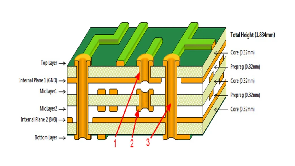
One recurring challenge involves balancing reduced environmental footprint with the stringent loss requirements of millimeter-wave or high-data-rate applications. Some sustainable resins exhibit slightly higher loss tangents, necessitating shorter trace lengths or alternative routing strategies. Engineers address this by incorporating simulation tools that model both material properties and layout geometry. High-frequency recyclable PCB solutions often combine selective use of sustainable layers with conventional materials in hybrid stack-ups where performance demands are highest.
Another consideration is long-term reliability under mechanical and thermal stress. Recyclable formulations must demonstrate consistent performance after multiple thermal excursions. Standardized qualification testing helps confirm that these materials meet the same acceptance criteria applied to conventional boards. When issues arise, root-cause analysis focuses on material lot variation, process parameters, or design features rather than assuming inherent limitations of sustainable options.
Conclusion
Recyclable PCB materials present a viable route for high-speed designs when electrical, thermal, and mechanical requirements receive equal attention during selection. Structured evaluation against established performance metrics enables teams to adopt sustainable options without compromising signal integrity. Continued refinement of material formulations and qualification methods will likely expand the range of applications where these choices become standard practice.
FAQs
Q1: What defines a recyclable PCB suitable for high-speed design?
A1: A recyclable PCB for high-speed applications uses substrate materials that support recovery processes while maintaining low dielectric loss and stable impedance characteristics across operating frequencies. Engineers verify these properties through standardized electrical testing and thermal cycling to ensure performance remains consistent with design targets.
Q2: How do sustainable PCB materials affect signal integrity in high-frequency circuits?
A2: Sustainable PCB materials performance depends on achieving comparable loss tangent and dielectric constant values to conventional options. Proper stack-up design, controlled copper distribution, and adherence to IPC-6012E qualification requirements help preserve signal integrity when transitioning to recyclable formulations.
Q3: Can recyclable materials meet the same reliability standards as traditional high-speed boards?
A3: Yes, when material selection follows IPC-A-600K acceptability criteria and includes appropriate environmental stress testing. Teams confirm that thermal expansion, moisture resistance, and mechanical strength align with application demands before production release.
Q4: What steps help evaluate recyclable options for a new high-speed project?
A4: Begin with electrical parameter targets, then review material datasheets for compatibility with fabrication and assembly processes. Prototype builds undergo signal integrity measurements and reliability testing to validate performance before scaling to volume manufacturing.





