 ALLPCB


Introduction
The PCB drilling process forms a critical foundation in printed circuit board manufacturing, enabling electrical interconnections and component mounting. Precision drilling creates vias for interlayer signal transmission and holes for through-hole components, directly influencing board performance and reliability. In high-density designs, achieving exact hole dimensions and positions becomes essential to support advanced electronics. Factory operations prioritize controlled parameters to minimize variations during mechanical or laser drilling. This article explores key techniques for via and component holes, focusing on engineering principles and manufacturing insights aligned with industry standards.
Understanding PCB Drilling and Its Importance
PCB drilling involves mechanically or optically removing material to form conductive pathways and mounting sites. Vias connect copper layers, while component holes accommodate leads for soldering. Poor drilling compromises signal integrity, assembly yield, and long-term durability in electric applications. Manufacturers stack panels for efficiency, drilling multiple boards simultaneously to optimize throughput. Adhering to standards like IPC-6012 ensures qualification for rigid boards, specifying performance criteria for hole quality.
Drilling precision matters because even minor deviations affect plating uniformity and impedance control. In multilayer boards, vias must align perfectly across layers to prevent open circuits. Component holes demand tight tolerances for press-fit or solder reliability. Factory-driven processes integrate drilling with subsequent steps like desmear and plating. Engineers specify drill files in Gerber format, detailing sizes and positions for CNC machines.
Key Technical Principles in PCB Drilling
PCB Drill Bit Types and Selection
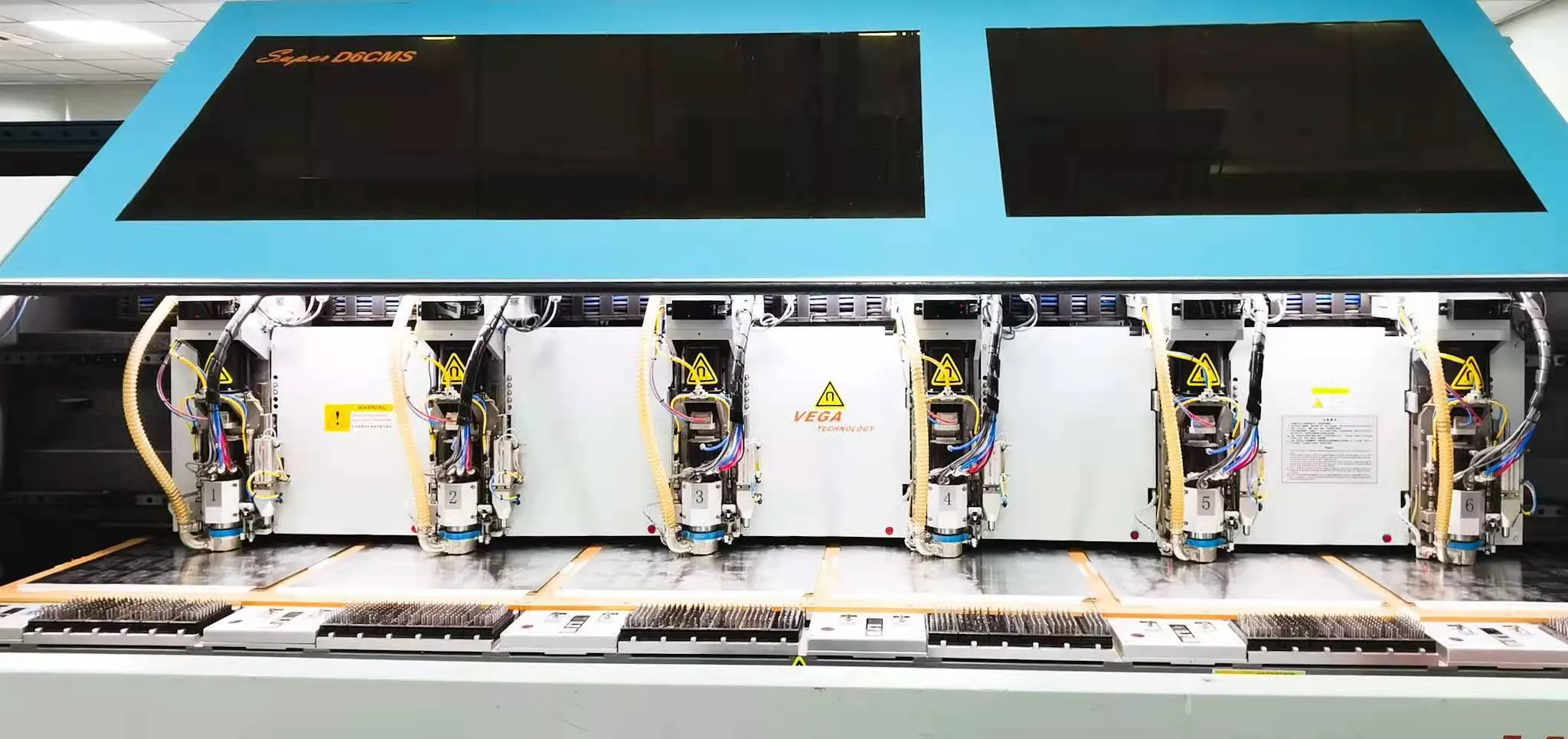
PCB drill bit types vary by hole size, board material, and application demands. Standard twist drills suit larger component holes, featuring helical flutes for chip evacuation. Undercut or fishbone designs enhance entry and reduce peel-back on copper layers. Micro drills, often under 0.15 mm, target fine-pitch vias in high-density interconnects. Tungsten carbide construction provides durability against abrasive fiberglass in FR-4 laminates. Selection depends on stack height and aspect ratio, with routers used for oversized holes or slots.
Factory experts match bit geometry to material properties for optimal cut quality. Straight flute bits minimize wandering in thin stacks, while multifaceted tips improve centering. Regrinding extends life but requires geometry checks to avoid defects. Engineers consider flute length for deep vias, ensuring effective debris removal.
Optimizing Drill Speed PCB Parameters
Drill speed PCB settings balance productivity and hole integrity. Spindle rotation, typically in tens of thousands of RPM, generates heat managed by coolant or air blasts. Feed rate advances the bit per revolution, influencing surface roughness. Retract speed clears chips rapidly to prevent clogging. Parameters adjust for laminate type, with higher speeds for epoxy resins versus ceramics.
Material hardness dictates adjustments; softer cores allow faster feeds. Stack count increases effective depth, slowing feeds to control breakthrough. Real-time monitoring via force sensors refines parameters dynamically. Consistent drill speed PCB practices reduce bit wear and maintain repeatability across production runs.
Achieving Drilling Accuracy in Production
Drilling accuracy encompasses positional tolerance, hole size variation, and wall roughness. CNC machines use fiducials for panel registration, achieving sub-micron repeatability. Optical alignment systems verify drill entry before plunging. Aspect ratios up to 10:1 challenge deeper boards, risking taper or bell-mouthing. IPC-A-600 defines acceptability criteria for hole features in class 2 and 3 products.
Vibration control via rigid spindles and entry materials preserves drilling accuracy. Thermal expansion in panels requires compensated tooling. Post-drill inspection with automated optical systems flags outliers. Factory protocols include pilot drilling for large holes, stepping to final size.
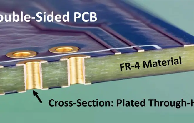
Hole Plating PCB After Drilling
Hole plating PCB transforms insulating holes into conductive vias post-drilling. Desmear removes epoxy smear from walls using plasma or permanganate etch. Electroless copper deposits a thin seed layer chemically, activating non-conductive surfaces. Electrolytic plating builds thickness, typically 25 microns or more, for current carrying.
Uniform coverage demands clean hole walls free of defects. Barrel integrity prevents cracks under thermal cycling. Sequential processes ensure plating adheres across aspect ratios. Engineers design annular rings per IPC guidelines to support plating growth.
Best Practices for Precision Drilling
Implement entry and backup materials to control drill entry and exit. Aluminum or phenolic entry minimizes bit wander, while foils prevent breakout. Vacuum extraction removes dust, preventing contamination. Panel fixturing ensures flatness during multi-hit cycles.
Optimize sequences by grouping similar sizes, reducing tool changes. Peck drilling for deep holes clears chips incrementally. Calibration routines verify spindle runout below 5 microns. Data analytics track bit life, scheduling replacements proactively.
Identifying and Preventing Drilling Defects
Drilling defects like burrs, rough walls, and nail heading arise from suboptimal parameters. Burrs form from inadequate feeds, protruding copper at entry. Roughness stems from dull bits or poor chip evacuation, hindering plating. Nail heading deforms inner copper layers under thrust.
Breakout occurs on exit without backup, fraying fibers. Misregistration links to panel warp or fiducial errors. Prevention involves parameter tuning and process controls. Regular bit inspection and coolant maintenance mitigate wear-related issues.
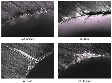
Factory troubleshooting uses cross-sections for root cause analysis. Adjusting drill speed PCB reduces heat-induced smear. Cleaner walls via desmear enhance hole plating PCB success. Standards guide defect limits, ensuring yield.
Conclusion
Precision in the PCB drilling process underpins reliable via and component hole formation. Selecting appropriate PCB drill bit types, tuning drill speed PCB, and upholding drilling accuracy drive quality. Effective hole plating PCB follows clean drilling, while proactive defect management sustains production. Factory insights emphasize standard-aligned practices for electric engineering demands. Mastering these techniques elevates board performance in demanding applications.
FAQs
Q1: What are the main PCB drill bit types used for vias and component holes?
A1: Standard twist, undercut, and micro drills form the core PCB drill bit types. Twist bits handle general holes, undercut designs reduce copper tear-out, and micro bits target fine vias. Selection aligns with hole size and material, ensuring clean cuts for plating. Factory processes regrind bits to maintain geometry.
Q2: How does drill speed PCB affect drilling accuracy?
A2: Drill speed PCB influences chip formation and heat generation, directly impacting drilling accuracy. Higher speeds enhance productivity but risk vibration if unmatched to feed. Balanced parameters prevent taper and roughness. Monitoring maintains positional tolerances per standards.
Q3: What causes common drilling defects in PCB manufacturing?
A3: Drilling defects like burrs and smear result from dull bits, improper feeds, or poor evacuation. Nail heading deforms copper under excessive thrust. Prevention involves optimized parameters and entry materials. Clean holes support reliable hole plating PCB.
Q4: Why is hole plating PCB critical after drilling?
A4: Hole plating PCB deposits copper for conductivity in vias and through-holes. Electroless seeding ensures adhesion on desmeared walls. Uniform plating prevents voids and cracks. It completes the interconnection path essential for multilayer functionality.
References
IPC-6012E — Qualification and Performance Specification for Rigid Printed Boards. IPC, 2017
IPC-A-600K — Acceptability of Printed Boards. IPC, 2020
IPC-2221B — Generic Standard on Printed Board Design. IPC, 2012


