In the fast-evolving world of electronics, precision and efficiency in manufacturing processes are more critical than ever. One technology that stands out in this domain is PCB Direct Imaging, particularly in the realm of IC substrate manufacturing. If you're wondering how IC substrate direct imaging transforms the production of high-density interconnects or what role LDI PCB manufacturing plays in creating intricate circuits, you've come to the right place. This blog will dive deep into the significance of PCB Direct Imaging, its impact on new technology IC substrate production, and why it’s a game-changer in PCB manufacturing and circuit creation.
At its core, PCB Direct Imaging, often implemented through Laser Direct Imaging (LDI), allows manufacturers to create highly precise circuit patterns directly on substrates without traditional photomasks. This leads to faster production cycles, reduced errors, and the ability to handle the complex demands of modern IC substrates. Let’s explore this technology in detail, breaking down the process PCB steps and its benefits for engineers and manufacturers alike.
What is PCB Direct Imaging and Why Does It Matter?
PCB Direct Imaging is a cutting-edge technique used in the production of printed circuit boards (PCBs) and IC substrates. Unlike traditional methods that rely on physical photomasks to transfer circuit patterns, direct imaging uses digital data to guide a laser or other imaging source to expose photosensitive materials on the substrate. This approach is particularly valuable in IC substrate direct imaging, where precision down to the sub-micron level is often required.
The importance of this technology cannot be overstated. As electronic devices become smaller and more powerful, the demand for high-density interconnect (HDI) boards and ultra-fine line circuits increases. With LDI PCB manufacturing, manufacturers can achieve line widths and spacing as narrow as 10 micrometers, ensuring that even the most complex designs are realized with accuracy. This precision is vital for IC substrates, which serve as the critical connection between semiconductor chips and the larger PCB, handling high-speed signals often exceeding 10 GHz in modern applications.
The Role of LDI in IC Substrate Manufacturing
IC substrates are the backbone of semiconductor packaging, acting as an intermediary between the IC chip and the main PCB. These substrates must support fine-pitch components and high-speed signal transmission, often requiring multiple layers with intricate via structures. This is where LDI PCB manufacturing shines, offering unmatched precision and flexibility in the process PCB creation.
Using Laser Direct Imaging, manufacturers can directly expose circuit patterns onto photosensitive layers of the substrate. This eliminates the need for traditional photolithography masks, which can introduce alignment errors and increase production time. With LDI, the digital design file is translated directly into a physical pattern, ensuring that even the tiniest features—down to 5 micrometers in some advanced systems—are accurately rendered. This capability is crucial for producing substrates that support high-performance applications like 5G, artificial intelligence, and automotive electronics.
Moreover, LDI allows for rapid prototyping and adjustments. If a design change is needed, there’s no need to create a new mask—just update the digital file, and the imaging system adapts instantly. This agility is a significant advantage in the fast-paced world of new technology IC substrate development, where time-to-market can make or break a product launch.
Key Benefits of PCB Direct Imaging in Circuit Creation
The adoption of PCB Direct Imaging in PCB manufacturing and circuit creation offers several benefits that directly impact quality, cost, and efficiency. Here are some of the standout advantages:
- Enhanced Precision: As mentioned earlier, LDI systems can achieve resolutions that traditional methods struggle to match. This is essential for IC substrates, where even a 1-micrometer deviation can disrupt signal integrity at high frequencies, such as those above 5 GHz.
- Reduced Production Time: By eliminating the need for physical masks, LDI cuts down on setup time. What used to take days in mask preparation can now be done in hours, speeding up the overall process PCB timeline.
- Cost Efficiency: While the initial investment in LDI equipment can be significant, the long-term savings are substantial. There’s no recurring cost for mask production, and the reduction in errors means less material waste.
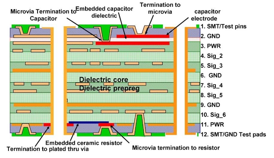
- Flexibility for Complex Designs: Modern IC substrates often feature multi-layer designs with blind and buried vias. LDI handles these complexities effortlessly, ensuring that each layer is aligned with precision, even in boards with over 10 layers.
- Environmental Benefits: Traditional photolithography involves chemical-intensive processes for mask creation and disposal. LDI reduces the chemical footprint, aligning with sustainable manufacturing goals.
Understanding the Process: How PCB Direct Imaging Works
To fully appreciate the impact of IC substrate direct imaging, it’s helpful to understand the step-by-step process of how LDI is applied in manufacturing. Here’s a breakdown of the process PCB creation using this technology:
- Design Data Preparation: The process begins with a digital design file, typically in a format like Gerber or ODB++. This file contains all the information about the circuit layout, including line widths, spacing, and via placements.
- Substrate Preparation: The IC substrate, often made of materials like BT resin or polyimide, is coated with a photosensitive resist layer. This layer will react to the laser exposure to form the circuit pattern.
- Laser Imaging: The LDI system uses a high-precision laser to expose the resist layer based on the digital design. The laser can adjust dynamically to create ultra-fine lines, often achieving resolutions below 10 micrometers.
- Development and Etching: After imaging, the substrate undergoes a development process to remove unexposed resist, revealing the desired pattern. This is followed by etching, where unprotected copper is removed to form the actual circuit traces.
- Inspection and Testing: Advanced optical inspection systems verify the accuracy of the pattern, checking for defects like shorts or opens. Electrical testing ensures signal integrity, especially critical for high-speed applications where impedance must be controlled within ±5% of the target value (e.g., 50 ohms for many RF designs).
This streamlined process not only enhances accuracy but also supports the iterative nature of modern design workflows, making it ideal for new technology IC substrate production.
Applications of PCB Direct Imaging in Modern Electronics
The versatility of PCB Direct Imaging makes it indispensable across various industries. In the context of IC substrate direct imaging, here are some key applications where this technology is driving innovation:
- 5G Technology: The rollout of 5G networks demands substrates that can handle frequencies up to 28 GHz and beyond. LDI ensures the precision needed for tight impedance control and minimal signal loss in these high-frequency designs.
- Automotive Electronics: With the rise of electric vehicles and autonomous driving, IC substrates must support complex sensor arrays and processing units. LDI enables the creation of reliable, high-density circuits for these safety-critical systems.
- Consumer Electronics: Smartphones, wearables, and IoT devices require compact, multi-layer substrates. LDI’s ability to produce fine-pitch patterns supports the miniaturization trend in these products.
- Artificial Intelligence and Data Centers: AI hardware and server-grade PCBs rely on substrates that can manage massive data throughput. LDI facilitates the intricate designs needed for high-speed signal routing, often exceeding 25 Gbps per channel.
Challenges and Future Trends in IC Substrate Direct Imaging
While LDI PCB manufacturing offers numerous advantages, it’s not without challenges. The high initial cost of LDI equipment can be a barrier for smaller manufacturers, though the return on investment often justifies the expense over time. Additionally, as designs push toward even finer resolutions—below 5 micrometers—LDI systems must evolve to maintain accuracy without sacrificing throughput.
Looking ahead, the future of new technology IC substrate production is bright. Advances in laser technology, such as the use of UV lasers with shorter wavelengths, promise even higher resolutions. Integration with AI and machine learning could further optimize imaging processes, predicting and correcting potential defects in real-time. Moreover, as the industry moves toward sustainable practices, LDI’s reduced chemical usage will likely become an even more significant selling point.
How PCB Direct Imaging Boosts Manufacturing Efficiency
Efficiency is the name of the game in PCB manufacturing and circuit creation. By adopting PCB Direct Imaging, manufacturers can streamline their workflows in ways that traditional methods can’t match. For instance, the elimination of mask-related steps reduces production bottlenecks, allowing for faster turnaround times—often cutting lead times from weeks to days. This is especially beneficial in industries where rapid prototyping is essential.
Furthermore, the precision of LDI minimizes rework and scrap rates. In high-volume production, even a 1% reduction in defective boards can translate to significant cost savings. When dealing with IC substrates, where material costs are high due to specialized laminates, this efficiency directly impacts the bottom line.
Conclusion: The Future of IC Substrate Manufacturing with Direct Imaging
PCB Direct Imaging, particularly through LDI PCB manufacturing, has redefined the landscape of IC substrate production. Its ability to deliver unparalleled precision, reduce production times, and support the complex demands of modern electronics makes it an essential tool for manufacturers. As the industry continues to push the boundaries of miniaturization and performance, technologies like IC substrate direct imaging will play a pivotal role in shaping the future of new technology IC substrate designs.
Whether you’re an engineer designing the next generation of 5G hardware or a manufacturer looking to optimize your process PCB workflow, understanding and leveraging PCB Direct Imaging can provide a competitive edge. This technology isn’t just a trend—it’s a cornerstone of innovation in PCB manufacturing and circuit creation, ensuring that the electronics of tomorrow are built on a foundation of precision and efficiency.
 ALLPCB


