 ALLPCB


If you're facing solder mask thickness deviation on your printed circuit board (PCB), you're not alone. This common issue can lead to uneven protection of copper traces, potential short circuits, and assembly problems. The good news? It can be managed with the right approach. In this comprehensive guide, we'll explore what solder mask thickness deviation is, why it happens, and how to address it effectively to ensure your PCB performs reliably.
What Is a PCB and Why Does Solder Mask Matter?
Before diving into the specifics of solder mask thickness, let's clarify what a PCB is. A printed circuit board is the backbone of electronic devices, providing a platform to connect and support electronic components like resistors, capacitors, and chips. It consists of layers of insulating material with conductive copper traces that form the electrical pathways.
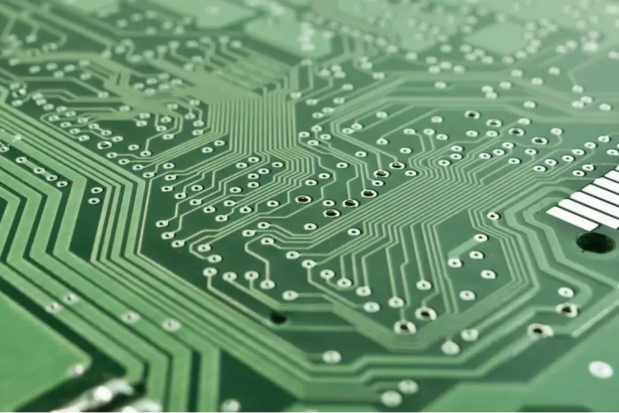
The solder mask is a thin protective layer, often green in color (though other colors like blue, red, or black are also used), applied over the copper traces on a PCB. Its primary role is to shield the copper from oxidation, prevent solder bridges during assembly, and protect against environmental damage like moisture or dust. When the solder mask thickness deviates—meaning it's uneven or not within the specified range—it can compromise these protective functions, leading to performance issues or even board failure.
Understanding Solder Mask Thickness and Its Importance
Solder mask thickness refers to the depth of the protective coating applied to the PCB. Typically, the standard thickness ranges from 0.8 to 1.2 mils (20 to 30 micrometers) on the copper traces and slightly thinner over the board's surface. Maintaining consistent thickness is crucial because:
- Protection: A uniform solder mask prevents corrosion and damage to copper traces.
- Insulation: It acts as an insulator, preventing unintended electrical connections or short circuits.
- Solderability: Consistent thickness ensures proper solder application during assembly, avoiding issues like solder bridging.
When thickness deviates—either too thick or too thin—it can cause problems. For instance, a mask that's too thin may not protect the copper adequately, leading to oxidation. Conversely, a mask that's too thick might interfere with component placement or soldering precision.
Common Evenness Problems with PCB Solder Mask
Evenness problems with PCB solder mask occur when the layer isn't applied uniformly across the board. This can manifest in several ways:
- Uneven Thickness: Some areas of the board may have a thicker or thinner mask due to inconsistent application.
- Bubbles or Voids: Air pockets or incomplete coverage can leave copper traces exposed.
- Misalignment: The solder mask may not align properly with the copper pads, exposing areas that should be covered or covering areas meant for soldering.
- Peeling or Cracking: Poor adhesion or curing can cause the mask to peel off, often due to uneven thickness during application.
These issues not only affect the board's appearance but also its functionality. For example, exposed copper can oxidize, increasing electrical resistance and potentially causing signal integrity issues, especially in high-frequency applications where impedance control is critical (e.g., maintaining 50 ohms for RF signals).
Causes of Solder Mask Thickness Deviation
Understanding why solder mask thickness deviation happens is the first step to addressing it. Several factors during the manufacturing process can contribute to this issue:
1. Inconsistent Application Methods
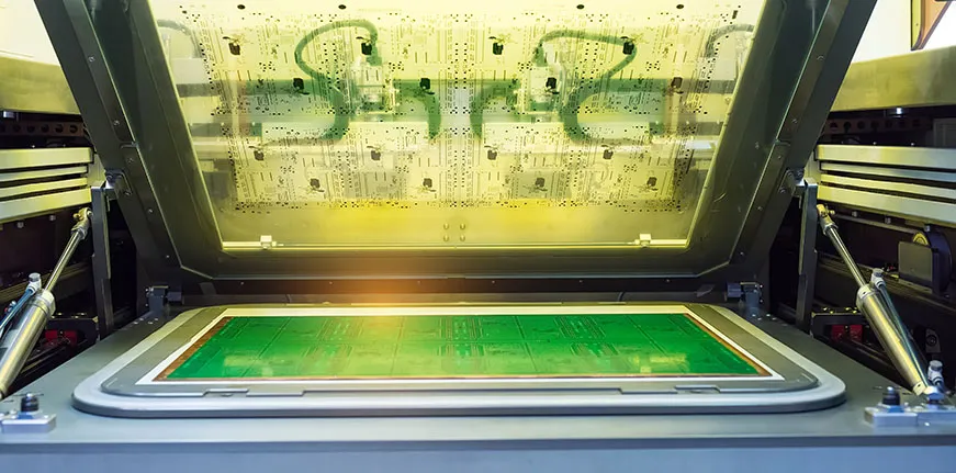
The solder mask is typically applied using methods like screen printing, curtain coating, or spray coating. If the equipment isn't calibrated correctly or the process parameters (like pressure or speed) aren't controlled, the thickness can vary across the board.
2. Material Quality Issues
The solder mask material itself—usually a liquid photoimageable polymer—must be of high quality. If the material has inconsistencies, such as varying viscosity, it can lead to uneven application. For instance, a viscosity outside the recommended range of 150-200 centipoise can cause flow issues during coating.
3. Improper Curing Conditions
After application, the solder mask is cured using heat or UV light to harden it. If the curing temperature (typically 120-150°C) or exposure time isn't uniform, some areas may not set properly, leading to thickness variations or adhesion problems.
4. Surface Contamination
Before applying the solder mask, the PCB surface must be clean. Dust, oil, or residue on the board can prevent the mask from adhering evenly, resulting in thin spots or voids.
5. Design and Layout Challenges
The PCB design itself can contribute to thickness deviation. For example, densely packed traces or varying copper heights (due to different trace widths, often ranging from 4 to 10 mils) can cause uneven mask distribution during application.
How to Identify Solder Mask Thickness Deviation
Detecting solder mask thickness issues early can save time and cost during PCB production. Here are some practical ways to identify deviations:
- Visual Inspection: Look for discoloration, bubbles, or areas where copper is visible through the mask. Uneven gloss or matte finishes can also indicate thickness issues.
- Microscopic Analysis: Use a microscope to measure thickness at multiple points on the board. Variations beyond ±10% of the target thickness (e.g., 0.8-1.2 mils) are a concern.
- Cross-Section Testing: Cut a small section of the PCB and examine the solder mask layer under a microscope to confirm uniformity.
- Electrical Testing: Check for unexpected resistance or short circuits, which may indicate exposed copper due to thin solder mask areas.
Solutions to Address Solder Mask Thickness Deviation
Now that we've covered the causes and identification methods, let's focus on actionable solutions to deal with solder mask thickness deviation on PCBs. These strategies span design, manufacturing, and quality control stages.
1. Optimize PCB Design for Uniform Application
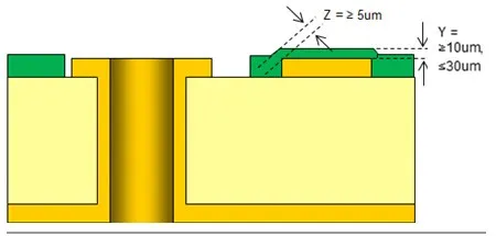
Start by designing your PCB with solder mask application in mind. Ensure that trace heights and densities are as uniform as possible to avoid uneven coating. For instance, maintain consistent trace widths (e.g., 6 mils for standard designs) and avoid abrupt changes in copper density. Additionally, include clear solder mask clearance specifications in your design files—typically 2-4 mils around pads—to prevent overlap or insufficient coverage.
2. Choose the Right Solder Mask Material
Select a high-quality solder mask material suited for your application. Liquid photoimageable solder masks are common for their precision, but ensure the viscosity and curing requirements match your manufacturing setup. Work with your manufacturer to verify material consistency before production begins.
3. Calibrate Application Equipment
Ensure that the equipment used for applying the solder mask—whether screen printing or spray coating—is properly calibrated. Regularly check parameters like roller pressure, nozzle speed, and material flow rate to maintain uniform application. For example, in screen printing, a mesh count of 100-120 threads per inch often provides consistent results for standard PCBs.
4. Control Curing Conditions
Monitor the curing process closely. Maintain a consistent temperature (e.g., 130°C for thermal curing) and exposure time across the entire board. If using UV curing, ensure the light intensity is uniform to avoid under-cured or over-cured areas that could affect thickness or adhesion.
5. Implement Strict Surface Preparation
Clean the PCB surface thoroughly before applying the solder mask. Use chemical cleaning agents or micro-etching to remove contaminants like oil or oxide layers. A clean surface ensures better adhesion and even distribution of the mask material.
6. Conduct Regular Quality Checks
Integrate quality control steps during and after production. Perform visual and microscopic inspections to catch thickness deviations early. Use automated optical inspection (AOI) systems if possible, as they can detect inconsistencies with high accuracy, often identifying defects smaller than 1 mil.
7. Collaborate with Your Manufacturer
Work closely with your PCB fabrication partner to address thickness deviation issues. Share detailed design files and specifications, and request feedback on potential manufacturing challenges. Many deviations can be minimized by aligning design intent with production capabilities.
Preventing Future Solder Mask Thickness Issues
Prevention is always better than correction. Here are some long-term strategies to minimize solder mask thickness deviation in future PCB projects:
- Standardize Processes: Develop a set of standard operating procedures (SOPs) for solder mask application and curing, ensuring consistency across production runs.
- Train Staff: Equip your team with training on proper equipment handling and quality control techniques to reduce human error.
- Update Equipment: Invest in modern application and inspection tools that offer better precision and automation, reducing the risk of unevenness.
- Test Prototypes: Before full-scale production, create and test prototypes to identify potential solder mask issues under real-world conditions.
The Impact of Solder Mask Thickness on PCB Performance
It's worth emphasizing how critical solder mask thickness is to overall PCB performance. For high-speed designs, an uneven solder mask can alter the dielectric constant, affecting signal propagation speeds (often measured in picoseconds per inch). In power electronics, inadequate protection from a thin mask can lead to arcing or breakdown under high voltages (e.g., above 500V). By addressing thickness deviations, you ensure not just reliability but also compliance with industry standards like IPC-A-600, which specifies acceptable solder mask coverage and thickness tolerances.
Conclusion
Dealing with solder mask thickness deviation on PCBs doesn't have to be a daunting task. By understanding what causes unevenness, identifying issues early through inspection, and applying targeted solutions like optimized design and controlled manufacturing processes, you can achieve a uniform and reliable solder mask layer. Consistent thickness—typically 0.8 to 1.2 mils—ensures your PCB is protected, functional, and ready for assembly.
Whether you're an engineer designing intricate boards or a manufacturer aiming for flawless production, addressing solder mask evenness problems is key to delivering high-quality electronics. With the tips and strategies outlined in this guide, you're well-equipped to tackle this common challenge and enhance the durability and performance of your PCBs.


