 ALLPCB


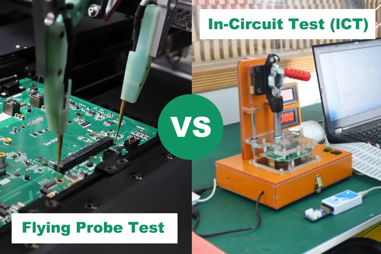
When it comes to ensuring the quality of printed circuit boards (PCBs), choosing the right testing strategy is crucial. Two popular methods, flying probe testing and bed-of-nails testing (often referred to as In-Circuit Testing or ICT), stand out as reliable options for detecting electrical issues like shorts, opens, and component failures. So, which one should you choose? In short, flying probe testing is ideal for low-volume production and prototypes due to its flexibility and lack of fixture costs, while bed-of-nails testing excels in high-volume manufacturing for its speed and cost-efficiency over large runs. In this blog, we’ll dive deep into a PCB testing methods comparison, exploring the advantages of flying probe testing and bed-of-nails testing to help you make an informed decision for your project.
Introduction to PCB Testing: Why It Matters
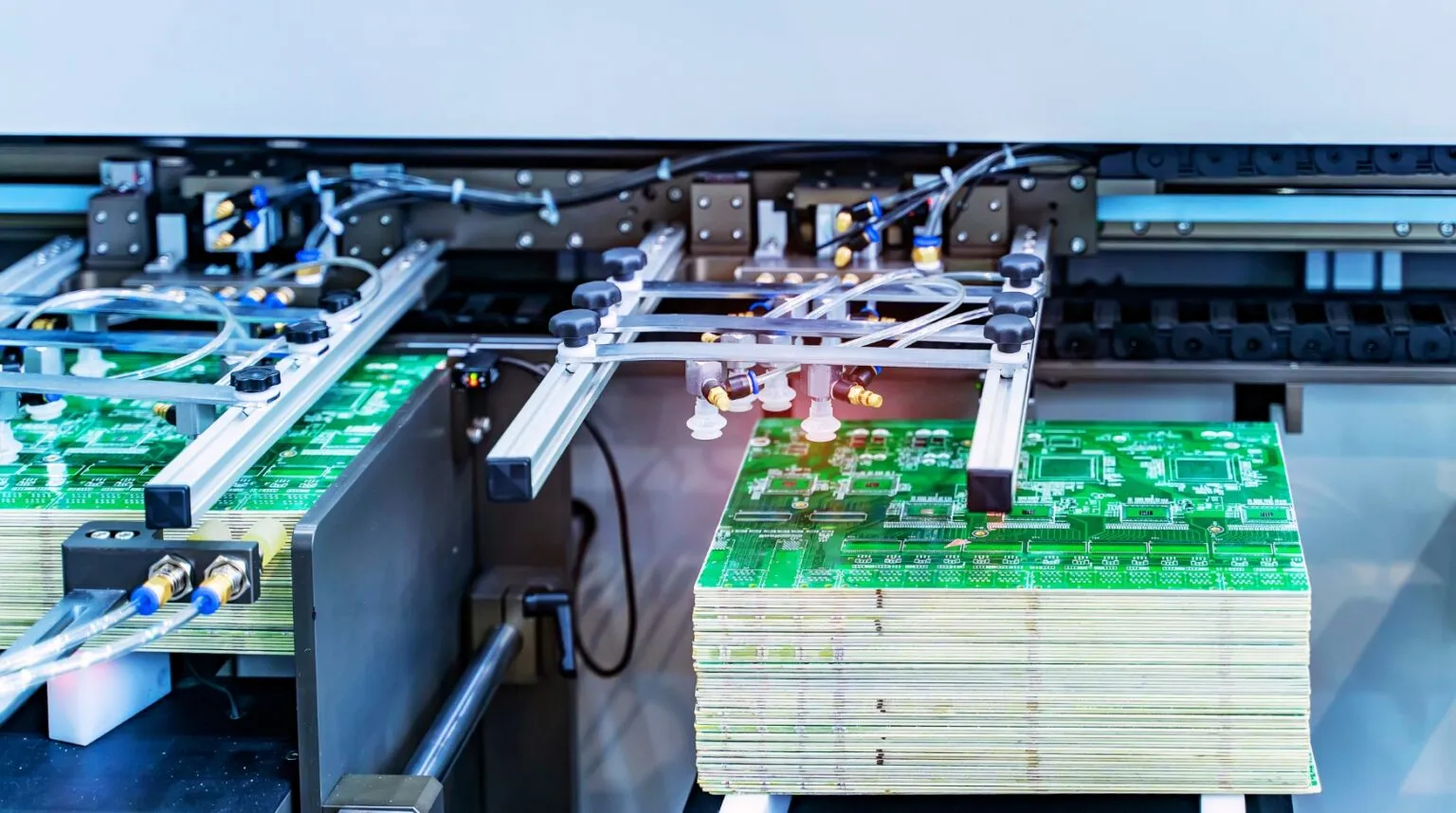
PCB testing is a critical step in the manufacturing process to ensure that every board functions as intended before it reaches the end user. Faulty boards can lead to product failures, costly recalls, and damaged reputations. Testing helps identify issues such as incorrect component placement, soldering defects, or broken connections early in the process. With the increasing complexity of modern electronics, selecting the right testing method can save time, reduce costs, and improve product reliability.
Two of the most widely used testing strategies are flying probe testing and bed-of-nails testing. Each method has unique strengths and weaknesses, making them suitable for different production scenarios. Whether you’re working on a small batch of prototypes or mass-producing thousands of boards, understanding the differences between flying probe testing vs ICT is essential. Let’s break down these methods in detail.
What Is Flying Probe Testing?
Flying probe testing is an automated, fixtureless method used to test the electrical performance of PCBs. Instead of relying on a fixed test fixture, this method uses movable probes that "fly" across the board to make contact with specific test points. These probes measure parameters like resistance, capacitance, and connectivity to detect faults such as shorts or opens.
The technology behind flying probe testing has evolved significantly. Modern systems can handle both bare boards and fully assembled PCBs, making them versatile for various stages of production. They are especially useful for quick-turn projects where design changes are frequent, as no custom fixtures are required.
How Flying Probe Testing Works
In a flying probe tester, multiple probes (usually 2 to 6) are programmed to move across the PCB based on the board’s design data. The probes touch specific test points to perform electrical measurements. For instance, a typical test might check for continuity between two points, expecting a resistance value of less than 1 ohm for a proper connection. If the measured resistance is significantly higher, it indicates a potential open circuit.
The process is slower compared to other methods because the probes must physically move to each test point. However, the lack of a physical fixture means setup time is minimal, often taking just a few hours to program the test based on the PCB layout.
What Is Bed-of-Nails Testing (In-Circuit Testing)?
Bed-of-nails testing, commonly known as In-Circuit Testing (ICT), uses a custom fixture filled with spring-loaded pins (the "nails") that align with test points on the PCB. When the board is pressed onto the fixture, the pins make contact with the test points, allowing the system to perform a wide range of electrical tests simultaneously. This method is designed to check for manufacturing defects like soldering issues, incorrect component values, and circuit faults.
ICT is a staple in high-volume production environments because it can test multiple points at once, drastically reducing test time per board. However, the need for a custom fixture means higher upfront costs and longer setup times, especially for new designs.
How Bed-of-Nails Testing Works
The bed-of-nails fixture is tailored to the specific PCB design, with pins positioned to match the board’s test points. Once the PCB is placed on the fixture, the system applies electrical signals through the pins to measure parameters like voltage, current, and resistance. For example, if a resistor on the board is supposed to have a value of 10 kΩ, the ICT system will measure its actual resistance and flag any deviation beyond a set tolerance, such as ±5%.
The test speed is impressive, often completing a full board check in just a few seconds. This makes it ideal for large production runs where thousands of identical boards need to be tested quickly.
Flying Probe Testing Advantages
Flying probe testing offers several benefits that make it a preferred choice for specific scenarios. Here are the key advantages:
- No Fixture Costs: Since flying probe testing doesn’t require a custom fixture, there are no upfront costs for designing and building a test bed. This can save thousands of dollars, especially for small runs or prototypes.
- Flexibility for Design Changes: If your PCB design changes frequently, flying probe testing adapts easily. The test program can be updated in hours without needing new hardware, unlike ICT which requires a new fixture for each design revision.
- Ideal for Low-Volume Production: For batches of fewer than 100 boards, flying probe testing is often more cost-effective due to the lack of fixture expenses and minimal setup time.
- Access to Hard-to-Reach Points: The movable probes can access test points in tight spaces or on densely populated boards, which might be challenging for a fixed fixture to cover comprehensively.
These advantages make flying probe testing a go-to method for prototype development and small-scale projects where flexibility and cost savings are priorities.
Bed-of-Nails Testing Advantages
Bed-of-nails testing, or ICT, shines in high-volume manufacturing environments. Here are its primary benefits:
- High Speed: ICT can test an entire board in just a few seconds by contacting all test points simultaneously. This speed is unmatched by flying probe systems, which test points sequentially.
- Cost-Effective for Large Runs: While the initial fixture cost can range from $1,000 to $10,000 depending on complexity, this expense is offset in high-volume production (e.g., 1,000+ boards) where the per-board test cost drops significantly.
- Comprehensive Testing: ICT systems can perform a wide range of tests, including functional testing and component-level diagnostics, often detecting issues like a capacitor with an incorrect value of 10 μF instead of the specified 100 μF.
- Consistency: The fixed fixture ensures repeatable and reliable contact with test points, reducing the risk of errors due to probe misalignment.
These strengths position bed-of-nails testing as the better choice for manufacturers producing large quantities of identical boards with stable designs.
Flying Probe Testing vs ICT: A Detailed Comparison
To help you decide between flying probe testing and bed-of-nails testing, let’s compare them across several key factors:
1. Cost
Flying probe testing has lower initial costs since no fixture is needed. However, the per-board test cost is higher due to slower test times, often ranging from $0.50 to $2 per board depending on complexity. In contrast, ICT involves a high upfront fixture cost but reduces the per-board cost to as low as $0.10 for large runs.
2. Speed
Bed-of-nails testing is much faster, completing tests in 5-10 seconds per board, while flying probe testing can take 1-5 minutes per board, depending on the number of test points. For a board with 500 test points, ICT’s parallel testing approach offers a clear speed advantage.
3. Setup Time
Flying probe testing requires minimal setup, often just a few hours to program the test based on the PCB design file. ICT setup, including fixture design and fabrication, can take 2-4 weeks for a new design, making it less suitable for quick-turn projects.
4. Volume Suitability
Flying probe is best for low to medium volumes (under 100-500 boards), while ICT is optimized for high volumes (1,000+ boards) where the fixture cost can be amortized over many units.
5. Design Flexibility
Flying probe testing wins for projects with frequent design iterations since no hardware changes are needed. ICT requires a new fixture for each design change, adding cost and delay.
When to Choose Flying Probe Testing
Opt for flying probe testing if your project fits the following criteria:
- You’re working on prototypes or small batches (under 100 boards).
- Your design is still evolving, and changes are expected.
- Budget constraints prevent investing in a custom test fixture.
- The PCB has densely packed components or test points in hard-to-reach areas.
For example, a startup developing a new IoT device might use flying probe testing during the R&D phase to validate multiple design iterations without incurring fixture costs.
When to Choose Bed-of-Nails Testing
Choose bed-of-nails testing if your project matches these scenarios:
- You’re manufacturing large volumes (1,000+ boards) with a stable design.
- Speed is critical to meet production deadlines.
- You need detailed, component-level testing for complex assemblies.
For instance, a consumer electronics manufacturer producing 10,000 identical smart home devices would benefit from ICT’s speed and cost-efficiency over the long run.
Combining Both Methods for Optimal Results
In some cases, manufacturers use a hybrid approach, combining flying probe and bed-of-nails testing to leverage the strengths of both. For example, flying probe testing can be used during the prototype phase to validate designs without fixture costs. Once the design is finalized and production ramps up, ICT can take over for high-speed, large-scale testing. Additionally, flying probe systems can test areas of a PCB that are inaccessible to an ICT fixture, ensuring full coverage.
This combined strategy is particularly useful for complex boards with mixed production needs, balancing cost, speed, and flexibility.
Conclusion: Making the Right Choice for Your PCB Testing Needs
Choosing between flying probe testing and bed-of-nails testing depends on your production volume, budget, design stability, and timeline. Flying probe testing offers unmatched flexibility and cost savings for low-volume and prototype projects, making it a favorite for R&D teams. On the other hand, bed-of-nails testing, or ICT, dominates in high-volume manufacturing with its speed and long-term cost efficiency.
By understanding the advantages of flying probe testing and bed-of-nails testing, you can align your testing strategy with your project’s specific requirements. Whether you prioritize quick setup and adaptability or high-speed testing for mass production, there’s a method that fits your needs. At ALLPCB, we’re committed to supporting your PCB manufacturing journey with tailored solutions to ensure quality and reliability at every step.


