ALLPCB


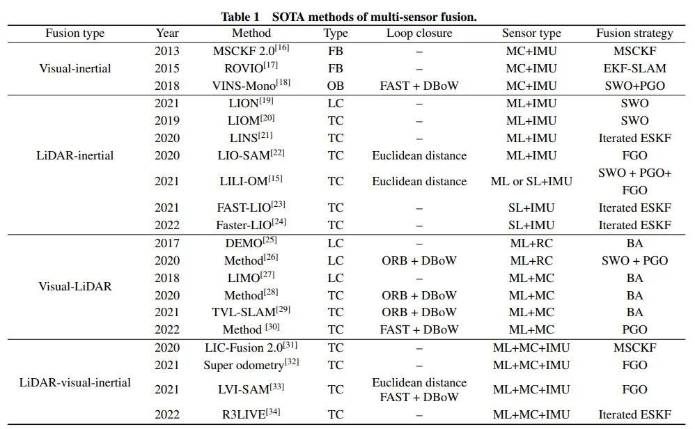
01 Basics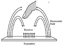
Capacitance is the ability of two conductive bodies separated by an insulating material to store charge. Capacitive sensing applies not only to human touch but also to detection of various materials and objects. According to the parallel-plate capacitance principle, the change in capacitance is proportional to electrode area and dielectric constant, and inversely proportional to the distance between electrodes.
Working principle: a capacitive sensor detects touch or proximity by measuring changes in capacitance between conductive bodies. When a finger or object approaches, the electric field distribution is altered, causing the capacitance to increase or decrease. This change can be represented by an equivalent circuit that includes multiple capacitance components.
Measurement method: capacitive sensing commonly uses a charge-transfer approach, repeatedly charging a sensing electrode and transferring charge to a sampling capacitor while counting transfer cycles. Observing changes in the required charging cycles reveals small capacitance variations. An analogy is filling a small container (variable capacitance) with liquid (charge) and pouring it into a larger container (fixed capacitance); the number of fills required reflects the small container’s capacity, and a change in that count indicates a capacitance change caused by touch or interaction.
02 Types and Applications
Self-capacitance vs mutual-capacitance: self-capacitance sensors monitor the capacitance of a single electrode relative to ground to detect touch. Mutual-capacitance sensors measure capacitance between a transmit electrode (Tx) and a receive electrode (Rx), supporting complex multi-touch.
Self-capacitance focuses on electrode-to-ground changes, typically in the 1–10 pF range. For large-area applications, a ring-shaped electrode can reduce overall capacitance and extend detection range, while small applications often use a single solid electrode for adequate detection.
Mutual-capacitance systems use separate Tx and Rx electrode structures connected to different microcontroller pins. When a finger contacts the intersection of Tx and Rx, it disturbs the field between them and reduces mutual capacitance, effectively introducing a grounded perturbation. The change in mutual capacitance is typically less than 1 pF.
03 Design Optimization Strategies
Design objective: sensor design must balance sensing range and system stability to improve sensitivity and accuracy. The goal is to maximize the touch-induced capacitance increment (CTouch) while minimizing parasitic capacitance. This requires careful electrode geometry and sizing, and selection of appropriate overlay materials and thicknesses.
Electrode design: electrode shape and area are critical for maximizing signal. Larger sensors provide greater coupling to the target and a wider sensing range. Unshielded proximity sensors can offer 360-degree detection, but interference from ground structures may reduce sensitivity.
Ground structures tend to concentrate field lines between the electrode and ground; it is necessary to limit field directions and prevent unwanted triggering. Ground shielding or driven shielding techniques can be employed.
Ground shielding: adding a grounded layer behind the sensor prevents the field from spreading rearward, but it shortens sensing distance because it introduces additional parasitic capacitance and absorbs field lines.
Driven shielding: a driven shield is a conductive layer placed beneath the sensor carrying the same drive signal as the sensor, typically implemented with an op amp configured as a voltage follower. When the shield’s drive is in phase and at the same potential as the sensor, no field forms between them. The shield also pushes the sensor field forward, reducing parasitic interference while preserving sensitivity to approaching objects, thereby improving signal-to-noise ratio.
Reducing parasitics and interference: to improve charge/discharge efficiency, electrodes and traces should use low-resistance materials. System parasitic capacitance attenuates the relative change caused by touch, making it harder to measure. For example, with 20 pF parasitic capacitance, a touch might produce a 25% change; with 100 pF parasitic capacitance, the same touch produces only a 5% change. To reduce parasitic effects, increase the distance between traces and ground planes and consider perforated ground patterns to optimize performance.
For large electrodes such as those used in proximity sensing, limit trace length to 120 mm and keep traces as narrow as practical. In mutual-capacitance systems, avoid routing Tx and Rx traces too close to each other to prevent reduced sensing distance.
Overlay: overlay design affects appearance and protection as well as sensitivity. Choose non-metallic overlays carefully. Overlay thickness and dielectric constant determine field coupling; using higher-dielectric-constant materials can mitigate the sensitivity loss caused by thick overlays. For air gaps or other low-dielectric situations, bridging materials improve coupling; effectiveness from best to worst: metal spring, conductive foam, carbon fiber, polycarbonate, ABS, silicone.
In self-capacitance applications, thinner overlays yield higher sensitivity. In mutual-capacitance designs, increasing overlay thickness moderately can sometimes improve sensitivity. Comparing materials, FPC exhibits relatively large temperature drift, while LDS technology shows smaller temperature drift.
Power supply method: supply type significantly affects proximity sensitivity, especially in battery-powered systems where coupling to earth is reduced. In a capacitive loop model, the sensor sees capacitances formed by the human body to sensor (C1), the electrode-to-module-to-earth path (C3, module-to-earth coupling), and the body-to-earth coupling (C2). When C3 is relatively small, C1’s detectability is weakened. For battery-powered systems, increasing the system ground area or providing a physical earth connection can improve coupling to earth and increase C3 to enhance detection performance.
AC mains-powered systems share earth ground and therefore generally show higher sensitivity. In well-grounded systems, the detection reference is more stable because module-to-earth coupling is effectively fixed, so small changes in C1 are easier to detect compared with battery-powered devices.
04 Challenges and Future Trends
Technical challenges: as devices trend toward thinner and lighter form factors, maintaining high capacitive sensing performance in constrained spaces is a major challenge. Power supply method impacts sensitivity and must be considered during design to optimize capacitance coupling and detection performance.
Future trends: driven by cost advantages, capacitive sensing is evolving toward higher sensitivity, smaller size, and lower power consumption, which will enable more applications and device innovations.
05 References
- Microchip Capacitive Proximity Design Guide
- CapTIvate Technology Guide - TI
- Capacitive Sensing Design Guide - Azoteq