ALLPCB


This article presents a waveguide embedded system (WES) based on optical printed circuit board technology for AI and HPC data centers, intended to address challenges in co-packaged optics (CPO) integration. WES integrates an optical engine with precision coupling structures to provide high-density, low-loss, fiberless device-to-device optical interconnects.
System Overview
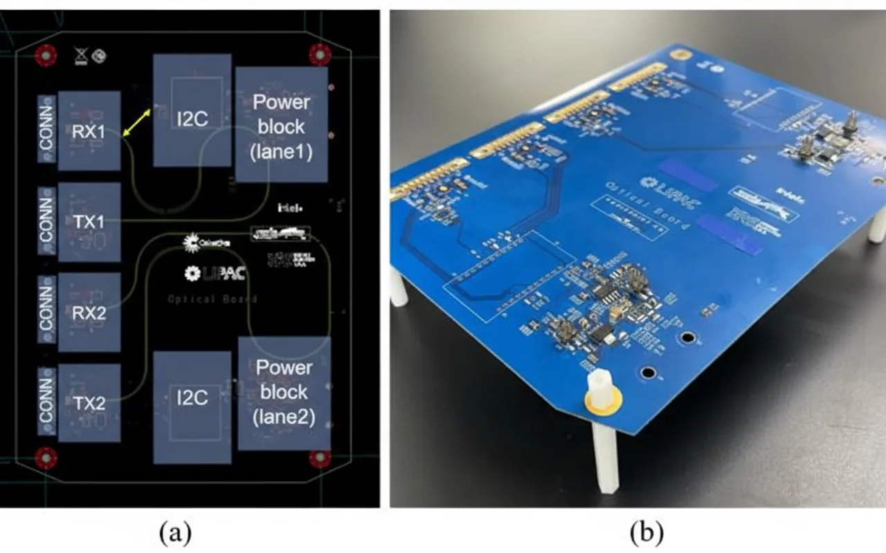
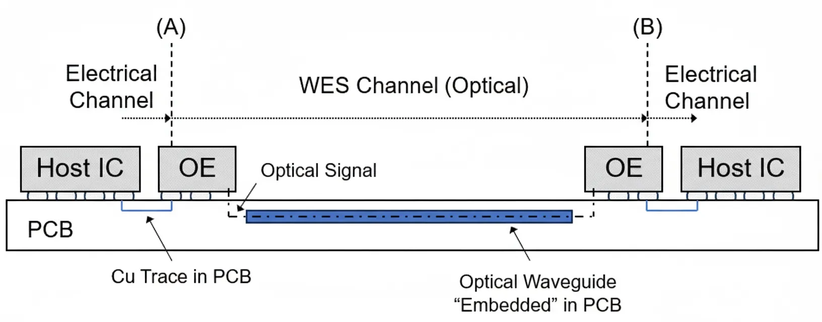
WES comprises three key components: the optical PCB, the optical engine, and the coupling structures. A WES channel converts electrical signals to the optical domain and back, enabling high-speed electrical data transfer from point A to point B. The optical channel is delivered by a highly integrated optical engine implemented as a semiconductor package and by embedded waveguides within the PCB to provide seamless data transfer.
A. Optical Engine
The terminals of a WES channel include an optical engine (OE) that converts electrical data to optical signals and vice versa. The OE includes VCSELs and driver ICs on the Tx side and photodiodes and TI A on the Rx side, connected by a short multimode waveguide.
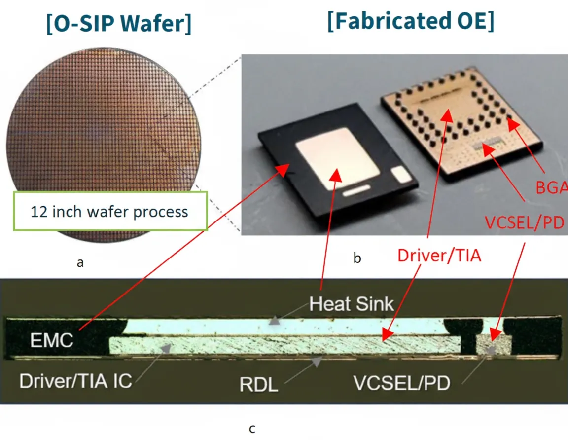
For seamless integration within a PCB ecosystem, the OE must have form factors comparable to other electrical components. Fan-out wafer-level packaging (FOWLP) is an advanced semiconductor packaging approach and a promising option for integrating VCSELs and photodiodes with electronic ICs. LIPAC introduced optical system-in-package (O-SiP) technology and supplied the optical engine used in this project.
B. Optical PCB
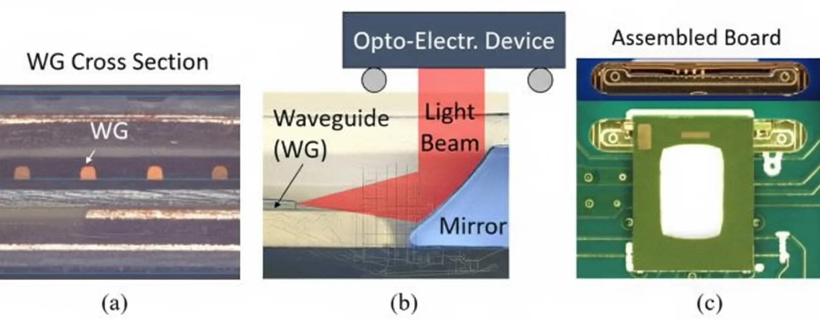
WES uses multimode waveguides embedded in the PCB as optical data channels. Similar to copper traces, waveguide layers can be arranged as interconnect traces and manufactured from polymer-based materials. The waveguide core can be formed by contact-mask photolithography or laser direct imaging (LDI), both compatible with conventional PCB fabrication. A 10–40 μm cladding layer is used to confine a 40–50 μm core layer, as shown in Figure 3(a).
C. Coupling Structures
Concave mirrors are used to couple light from OE-embedded VCSELs to Tx-side waveguides and from waveguides to OE-embedded photodiodes on the Rx side. As shown in Figure 3(b), beams are focused into the waveguide and photodiode. Alignment tolerances for the coupler are approximately ±15 μm in X-Y and ±40 μm in Z. The reflector assembly includes guiding features that mate with references in the waveguide layer, allowing the mirror assembly to be placed on the PCB and aligned precisely with the waveguide. Figure 3(c) shows the assembled mirror module on the PCB, which incorporates integrated waveguide structures fabricated from various optical elements. Other coupling approaches are possible; for example, microGlass proposed a dual-chip coupling structure, with one chip for the OE side and another for the PCB side, to improve alignment accuracy.
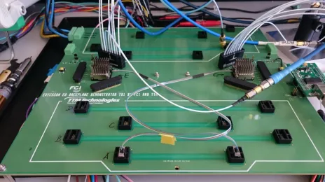
Demonstrator Assembly
Assembling OEs on the PCB requires higher placement accuracy than typical electrical components. Alignment tolerances are determined by the optical design of the coupling structure, so assembly methods must be chosen carefully. For the proof-of-concept demonstrator, a flip-chip bonder placed the OE on the PCB with a placement tolerance of ±5 μm. To enable use of conventional IR reflow, epoxy was applied between the PCB and OE before placement. The epoxy fixes the position achieved by the flip-chip bonder and prevents OE movement during IR reflow.