 ALLPCB


When designing a printed circuit board (PCB), every detail matters. Non-Plated Through-Holes (NPTH) are a critical element often overlooked, yet they play a vital role in ensuring mechanical stability and reliability. So, what are the key design rules for NPTH to achieve optimal performance? In short, focus on proper clearance, spacing, hole diameter, tolerance, annular rings, stack-up considerations, and impedance control where applicable. This blog post dives deep into these NPTH design rules, offering practical guidance for engineers aiming to enhance their PCB designs for durability and functionality.
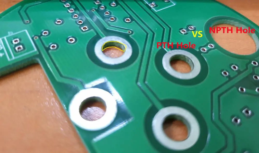
What Are Non-Plated Through-Holes (NPTH)?
Non-Plated Through-Holes are holes drilled through a PCB that do not have a conductive copper layer on their inner walls. Unlike Plated Through-Holes (PTH), which are used for electrical connections between layers, NPTH are typically used for mechanical purposes. These include mounting holes for screws, alignment pins, or as openings for components that don’t require electrical conductivity.
While NPTH may seem simple, improper design can lead to issues like mechanical failure, misalignment, or interference with nearby traces. Following strict design rules ensures these holes serve their purpose without compromising the PCB’s overall performance.
Why NPTH Design Rules Matter
Designing NPTH with precision is essential for several reasons. First, they ensure mechanical stability by providing secure mounting points. Second, they prevent interference with electrical signals by maintaining proper clearance from conductive traces. Finally, well-designed NPTH contribute to the overall reliability of the PCB, reducing the risk of cracks, misalignment, or manufacturing defects.
Let’s break down the specific design rules for NPTH, focusing on clearance, spacing, annular rings, hole diameter, tolerance, stack-up, and impedance control considerations.
1. Clearance: Keep Electrical and Mechanical Safety in Mind
Clearance refers to the minimum distance between an NPTH and the nearest copper trace, pad, or plane. Since NPTH are not conductive, they don’t pose a direct risk of short circuits. However, insufficient clearance can lead to manufacturing issues or mechanical stress that damages nearby traces.
A common guideline is to maintain a clearance of at least 0.2 mm (8 mils) between the edge of an NPTH and any copper feature. For high-voltage designs, this clearance may need to be increased to 0.5 mm (20 mils) or more to prevent arcing or dielectric breakdown. Always check the specific requirements of your design and manufacturing process to avoid costly errors.
2. Spacing: Avoid Overcrowding for Structural Integrity
Spacing is the distance between multiple NPTH or between NPTH and other features like vias or component pads. Proper spacing prevents structural weaknesses in the PCB material, especially in areas with multiple holes. A general rule is to keep a minimum spacing of 0.5 mm (20 mils) between NPTH edges. For larger holes or high-stress areas, consider increasing this to 1 mm (40 mils) to maintain board strength.
Spacing also affects manufacturing. If holes are too close, the drilling process can cause micro-cracks or delamination in the PCB substrate. Always balance the need for compact design with the structural demands of your board.
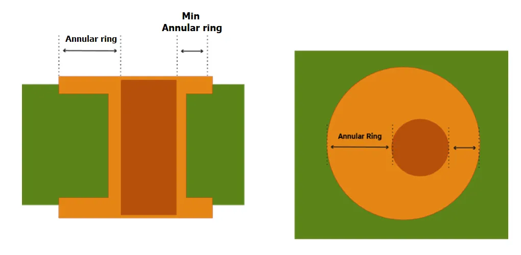
3. Annular Rings: Reinforce Mechanical Stability
Even though NPTH are not plated, they often require an annular ring—a ring of copper around the hole on the outer layers. This ring isn’t for conductivity but for mechanical reinforcement. It helps distribute stress from screws or fasteners, preventing the hole from cracking under pressure.
For NPTH, a minimum annular ring width of 0.15 mm (6 mils) is often recommended. However, for holes under heavy mechanical load, such as those for large screws, increase this to 0.3 mm (12 mils) or more. Ensure the annular ring is present on both the top and bottom layers if the hole is used for mounting.
4. Hole Diameter: Match Purpose and Manufacturing Limits
The diameter of an NPTH depends on its purpose. For mounting holes, the diameter should match the screw or fastener size, typically ranging from 2 mm to 5 mm (80 to 200 mils). For alignment pins or smaller mechanical features, diameters as small as 0.8 mm (32 mils) may suffice.
Keep in mind the manufacturing capabilities of your PCB fabricator. Most standard processes can handle NPTH diameters down to 0.5 mm (20 mils) with a tolerance of ±0.1 mm (4 mils). Smaller holes may require specialized drilling equipment, increasing costs. Always design within these limits unless your application demands precision beyond standard capabilities.
5. Tolerance: Account for Manufacturing Variations
Tolerance defines the acceptable variation in hole size and position during manufacturing. For NPTH, a typical tolerance for hole diameter is ±0.1 mm (4 mils), while positional tolerance is often ±0.05 mm (2 mils). Tight tolerances are critical for applications like mounting holes where precise alignment with enclosures or other components is necessary.
Over-specifying tolerances can drive up manufacturing costs. For instance, a tolerance of ±0.025 mm (1 mil) may require advanced drilling techniques. Evaluate whether your design truly needs such precision or if standard tolerances will suffice.
6. Stack-Up Considerations: Align with Board Layers
PCB stack-up refers to the arrangement of copper and insulating layers in a multi-layer board. While NPTH don’t conduct electricity, their placement must still align with the stack-up to avoid interfering with internal layers or causing manufacturing issues.
For example, ensure that NPTH don’t pass through critical internal power or ground planes unless absolutely necessary. If they must, maintain a clearance of at least 0.3 mm (12 mils) from internal copper to prevent accidental contact during drilling. Additionally, consider the board thickness when designing NPTH. Thicker boards (e.g., 2.4 mm or 94 mils) may require larger hole diameters or adjusted tolerances to account for drilling challenges.
7. Impedance Control: Indirect but Important
Impedance control is typically associated with high-speed signal traces, not NPTH. However, NPTH placement can indirectly affect impedance by altering the dielectric environment or interfering with nearby controlled-impedance traces. For instance, placing an NPTH too close to a high-frequency trace (e.g., one designed for 50 ohms impedance) can disrupt signal integrity due to changes in the effective dielectric constant.
To mitigate this, maintain a clearance of at least 0.5 mm (20 mils) between NPTH and any impedance-controlled traces. In designs operating at frequencies above 1 GHz, consider simulating the impact of NPTH placement using electromagnetic field solvers to ensure signal performance isn’t compromised.
Practical Tips for Implementing NPTH Design Rules
Designing NPTH for optimal performance requires more than just following rules—it demands practical application. Here are some actionable tips to help you integrate these guidelines into your workflow:
- Use Design Software Features: Leverage PCB design tools to set up design rule checks (DRC) for clearance, spacing, and annular rings. This automates error detection early in the design phase.
- Consult Manufacturer Guidelines: Different fabricators have varying capabilities for hole drilling and tolerances. Always review their design for manufacturability (DFM) rules before finalizing your NPTH specifications.
- Test Mechanical Fit: If NPTH are used for mounting, prototype the design with actual screws or fasteners to ensure proper fit and alignment.
- Consider Board Material: The PCB substrate (e.g., FR-4) affects drilling precision and mechanical strength. For high-stress NPTH, consider reinforced materials or thicker boards.
Common Mistakes to Avoid in NPTH Design
Even experienced engineers can make errors when designing NPTH. Here are some pitfalls to watch out for:
- Ignoring Clearance: Placing NPTH too close to traces can lead to manufacturing defects or signal interference, especially in dense designs.
- Overlooking Annular Rings: Skipping or undersizing annular rings can weaken mounting holes, causing cracks under mechanical stress.
- Specifying Unrealistic Tolerances: Demanding extremely tight tolerances without justification increases costs and delays without adding value.
- Poor Stack-Up Planning: Failing to account for internal layers during NPTH placement can result in unintended interference or structural issues.
How NPTH Design Impacts Manufacturing and Cost
The way you design NPTH directly affects the manufacturing process and overall project cost. For instance, smaller hole diameters or tighter tolerances often require specialized drilling tools, increasing production time and expense. Similarly, inadequate spacing or clearance can lead to higher defect rates, requiring costly rework.
To optimize costs, stick to standard hole sizes (e.g., 0.8 mm to 3 mm) and tolerances (±0.1 mm) unless your application demands otherwise. Additionally, group NPTH in areas that simplify drilling patterns, reducing setup time for manufacturers.
Conclusion: Mastering NPTH for Reliable PCB Designs
Non-Plated Through-Holes may not carry electrical signals, but they are just as important as any other PCB feature. By adhering to design rules for clearance, spacing, annular rings, hole diameter, tolerance, stack-up, and impedance control, you can ensure that NPTH contribute to the mechanical stability and overall reliability of your board.
Whether you’re designing a simple prototype or a complex multi-layer PCB, paying attention to these details will save time, reduce costs, and prevent failures down the line. Implement these guidelines in your next project to achieve optimal performance and durability.
At ALLPCB, we’re committed to supporting engineers with the tools and resources needed for successful PCB designs. Apply these NPTH design rules to create boards that stand the test of time.


