 ALLPCB


Introduction
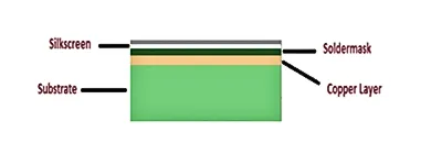
Single-layer PCB designs remain popular in cost-sensitive applications such as consumer electronics, sensors, and simple control circuits due to their simplicity and low fabrication costs. However, these single sided PCB noise reduction challenges arise prominently because of the absence of dedicated inner layers for ground planes or power distribution. PCB electromagnetic interference, or EMI, can degrade signal integrity, cause malfunction in nearby circuits, and lead to compliance failures in regulated environments. Engineers must employ targeted strategies to contain electromagnetic fields and provide low-impedance return paths within the constraints of a single copper layer. This article explores practical techniques grounded in engineering principles to minimize single layer PCB EMI effectively. By focusing on layout optimization and component strategies, designers can achieve reliable performance without escalating to multilayer boards.
Understanding EMI in Single-Layer PCBs and Why It Matters
Electromagnetic interference in PCBs manifests as radiated emissions from traces acting as antennas or conducted noise through power lines coupling into signals. In single-layer designs, the lack of a continuous ground plane forces all signals, power, and returns onto one side, amplifying loop areas that radiate EMI. This becomes critical for signal integrity, where high-frequency switching in digital circuits induces noise affecting analog sections or off-board communications. Poor EMI control can result in intermittent failures, increased susceptibility to external fields, and redesign iterations, inflating development costs. For electrical engineers, mastering single layer PCB EMI mitigation ensures robust designs that meet performance specs in compact, budget-limited projects. Ultimately, effective techniques preserve functionality while adhering to fundamental design principles.
Key Causes of EMI in Single-Layer Designs
The primary mechanisms driving PCB electromagnetic interference in single-layer boards stem from uncontrolled current return paths and field coupling. When signal traces lack an adjacent reference plane, return currents spread across distant ground traces, forming large loops that efficiently radiate magnetic fields at frequencies above a few MHz. Crosstalk exacerbates this as parallel traces couple capacitively and inductively, injecting noise into sensitive lines without shielding layers to contain fields. Component switching transients, such as from microcontrollers, generate broadband noise that propagates unchecked due to high-impedance ground paths. Edge effects further contribute, where traces near board edges act as slot antennas, leaking emissions. Understanding these causes allows engineers to prioritize interventions like loop minimization early in the design phase.
Technical Principles for EMI Control
Effective EMI suppression relies on confining electric and magnetic fields close to conductors, as per established transmission line theory. In single-layer PCBs, signals behave as unbalanced microstrips over air or substrate, with fields extending far without a ground reference, increasing radiation. Minimizing loop inductance follows from Ampere's law, where smaller enclosed areas reduce magnetic flux linkage and thus far-field emissions. Impedance discontinuities from varying trace widths or bends create reflections, amplifying noise spectra. Grounding techniques provide low-impedance returns, shunting high-frequency currents away from radiating structures. Signal integrity improves through controlled characteristic impedance, even if approximate, to match source and load, damping ringing. These principles guide layout decisions, ensuring currents follow intended paths rather than forming unintended antennas.
IPC-2221A outlines spacing and plane distribution to mitigate such field leakage, emphasizing even ground referencing along edges.
Grounding Techniques for Single-Layer PCBs
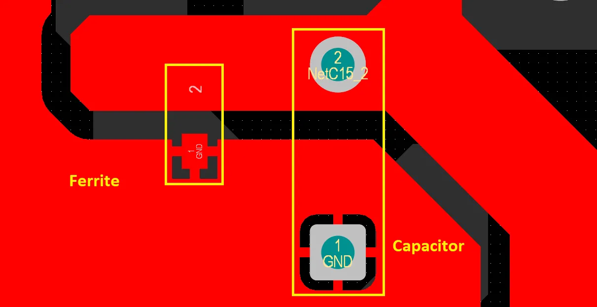
Grounding forms the cornerstone of single sided PCB noise reduction, compensating for the missing plane with strategic copper utilization. Dedicate the largest possible area to a continuous ground pour, connected via multiple vias or pads if through-hole components allow, to lower overall impedance. For microcontrollers or noisy ICs, create a local ground island extending slightly beyond the component outline, tying bypass capacitors directly to it for minimal loop areas. Employ star grounding by routing separate analog, digital, and power grounds to a single central point, preventing loops between domains. Widen all ground traces to at least 1.5 mm, running them parallel to signal lines to approximate a distributed return path. This configuration reduces common-mode noise and provides shielding against crosstalk.
Avoid narrow necks or jumps in ground paths, as they introduce inductance spikes. In practice, fill all unused board areas with grounded copper, stitching edges with short traces to form a grid-like structure. This not only aids heat dissipation but also captures stray fields, directing them to ground.
Optimizing Trace Routing and Component Placement
Trace routing profoundly impacts single layer PCB EMI by controlling loop geometry and coupling. Keep high-speed signals short, routing them away from board edges and using gentle 45-degree bends instead of right angles to minimize reflections and field concentrations. Maintain separation of at least three times the trace width between noisy digital lines and sensitive analog traces, grouping signals with adjacent ground guards where possible. Place decoupling capacitors within millimeters of IC power pins, with short, wide traces to ground forming PI filters if ferrite beads are added. Position noise sources like oscillators and switching regulators centrally or near power entry, isolating them from I/O connectors by at least one dielectric thickness.
Component placement follows zoning: cluster high-speed logic together, surround with ground, and distance low-speed or analog sections. Overlap power and ground traces directly to leverage inter-trace capacitance for bypassing.
IPC-2141A provides formulas for estimating microstrip impedance in such configurations, aiding signal integrity by matching trace width to substrate thickness.
Filtering, Shielding, and Additional Best Practices
Passive filtering suppresses conducted EMI at its source. Place 0.1 μF ceramic decoupling capacitors across every IC supply pin to ground, supplemented by 1000 pF for higher frequencies, ensuring vias or pads connect directly to the local ground island. Ferrite beads on power lines create high-impedance blocks for RF while passing DC, forming effective PI networks. For outputs, add series resistors (33-100 Ω) near the driver to dampen edge rates and reduce differential emissions.
Shielding via metal cans over critical areas connects to ground at multiple points for low-inductance paths. Terminate unused pins to ground, removing floating conductors that resonate as antennas. Simulate loop areas during layout review, targeting reductions below 1 cm2 for signals above 10 MHz. These layered approaches cumulatively lower emissions without multilayer complexity.
Troubleshooting Common EMI Issues
Engineers often encounter radiated peaks from clock harmonics or conducted noise on power rails during prototyping. Verify ground continuity with a multimeter at high frequencies using a scope's FFT mode, identifying high-impedance spots. If crosstalk appears, increase spacing or insert ground traces between victims and aggressors. For persistent edge radiation, add via fences or edge stitching with grounded pads. Iterative testing with near-field probes pinpoints sources, allowing targeted fixes like rerouting or extra bypassing. Document changes against baseline emissions to quantify improvements.
Conclusion
Minimizing EMI in single-layer PCB designs demands disciplined application of grounding techniques, precise routing, and proactive filtering to overcome inherent limitations. By maximizing ground areas, shrinking loops, and isolating domains, engineers achieve signal integrity and compliance in cost-effective boards. These strategies, rooted in electromagnetic principles, extend to more complex designs while emphasizing fundamentals. Implementing them early prevents costly respins, delivering reliable performance for electrical engineering applications. Prioritize simulation and prototyping to validate, ensuring robust single sided PCB noise reduction.
FAQs
Q1: How do grounding techniques improve single layer PCB EMI performance?
A1: Grounding techniques like wide pours and star points provide low-impedance returns, confining fields and reducing radiation loops. Local islands under ICs shunt switching noise effectively, while parallel ground-signal routing mimics planes. This lowers emissions and boosts signal integrity per IPC-2221A guidelines. Overall, they transform the single copper layer into an efficient EMI shield.
Q2: What role does trace routing play in PCB electromagnetic interference control?
A2: Optimal routing minimizes loop areas and crosstalk by keeping traces short, separated, and paralleled with grounds. Avoid edges and sharp bends to prevent antenna effects, using 3W spacing rules. Guard traces further isolate signals, preserving integrity in noise-prone environments. These practices directly cut radiated and conducted EMI.
Q3: Can single-layer boards achieve good signal integrity without multilayer stackups?
A3: Yes, through approximate impedance control via consistent widths and decoupling, alongside minimal loops. IPC-2141A microstrip equations guide trace sizing for better matching. Filtering and placement zoning compensate for absent planes, ensuring reliable high-speed operation in constrained designs.
Q4: What are essential steps for single sided PCB noise reduction during layout?
A4: Fill unused areas with ground pours, place decaps near pins, and zone components by noise profile. Route returns adjacent to signals, add series termination for edges, and verify with EMI probes. Shielding cans handle residual issues, yielding compliant boards efficiently.
References
IPC-2221A — Generic Standard on Printed Board Design. IPC, 2003
IPC-2141A — Design Guide for High-Speed Controlled Impedance. IPC, 2004


