 ALLPCB


Introduction
Miniaturization drives the electronics iNavigate the complexities of high density interconnect PCB assembly and precise component placement. Learn to tackle miniaturization challenges, from tiny part handling to thermal stress, ensuring robust and reliable electronics.ndustry forward, packing more functionality into smaller spaces through advanced printed circuit board designs. High-density-interconnect circuit boards represent a key enabler, featuring finer lines, microvias, and tighter component spacing to support compact devices like smartphones and wearables. However, PCB assembly faces significant hurdles when scaling down, from handling minuscule parts to ensuring reliable interconnections. These challenges demand precise processes to avoid defects that could compromise performance. Engineers must troubleshoot issues like misalignment and thermal stress proactively. This article explores the core difficulties and practical strategies for successful assembly.
Understanding High-Density-Interconnect Circuit Boards and Their Assembly Demands
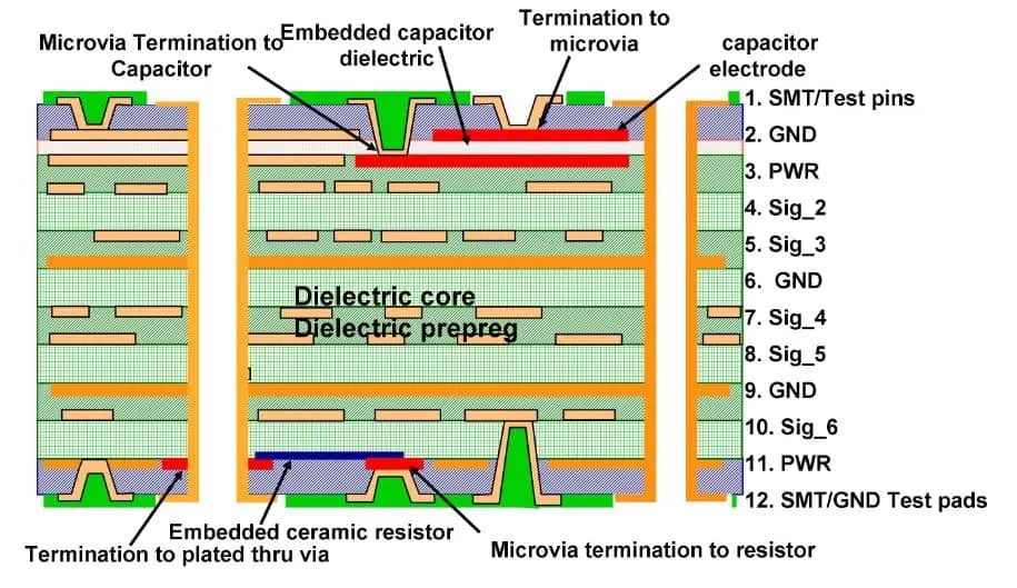
High-density-interconnect circuit boards use blind and buried vias along with laser-drilled microvias to achieve routing densities far beyond standard multilayers. This technology allows for more components in less area, but assembly requires adapting surface-mount technology to extreme tolerances. Components such as 0201 resistors or finer pitch BGAs challenge conventional pick-and-place systems with their reduced footprints. Solder paste deposition becomes critical, as stencil apertures must align perfectly to prevent bridging or insufficient volume. According to IPC-2226A, design rules for these boards emphasize via reliability and trace integrity under dense layouts. Assembly teams often encounter yield drops without optimized fixturing and process controls.
The push for miniaturization stems from consumer demands for sleeker products, yet it amplifies risks during reflow soldering. Thinner boards prone to warpage complicate uniform heating, leading to inconsistent joints. Precise component placement accuracy, typically under 50 microns for fine-pitch devices, tests machine vision and nozzle precision. Troubleshooting starts with verifying feeder alignment and vacuum grip on lightweight parts. High-density-interconnect circuit boards thus shift assembly from routine to highly specialized workflows.
Key Challenges in Precise Component Placement
Achieving precise component placement on miniaturized boards involves overcoming mechanical and optical limitations in automated equipment. Tiny parts like 01005 capacitors weigh fractions of a gram, making them susceptible to static charge or airflow displacement during transfer. Pick-and-place heads must maintain sub-25-micron accuracy, but vibration or substrate flex can cause offsets. Engineers troubleshoot by calibrating vision systems against fiducials and using high-resolution cameras for part recognition. In high-density-interconnect circuit boards, pad sizes shrink to match component leads, leaving no margin for error in alignment.
Solder paste volume inconsistencies exacerbate placement issues, as uneven deposits lead to tombstoning where one end lifts during reflow. Stencil printing demands laser-cut apertures with step-down features for ultra-fine pitches below 0.3mm. Jet printing offers an alternative for non-contact deposition, reducing smear risks on delicate surfaces. Practical fixes include pre-bake boards to minimize moisture and employ dual-lane feeders for continuous supply. Without these, rework cycles increase, delaying production.
Thermal Management and Mechanical Stress in Miniaturized Assemblies
Reflow profiles must balance rapid heating for lead-free solders with avoiding overheating thin copper layers in high-density-interconnect circuit boards. Peak temperatures near 260°C risk delamination if CTE mismatches between layers cause warpage. Boards under 0.8mm thick bow during cooling, misaligning components and stressing joints. Troubleshooting involves shadow moiré analysis to quantify warp and adjust conveyor supports. Nitrogen atmospheres help by reducing oxidation on fine-pitch leads.
Solder joint reliability suffers from voiding in micro-BGAs, where trapped flux gases expand under heat. Precise component placement ensures even standoff heights, but via-in-pad designs trap more air. Engineers mitigate this through extended preheat zones and low-voiding pastes. Mechanical shock testing per J-STD-001J reveals weaknesses early, guiding profile tweaks. These steps prevent field failures in vibration-prone applications.
Inspection and Quality Assurance Hurdles
Visual inspection fails for hidden joints in dense assemblies, necessitating automated optical and X-ray systems. AOI struggles with shadow effects from stacked components, missing bridges under 01005 parts. X-ray reveals voids or head-in-pillow defects, but throughput lags for high-volume runs. Calibration against IPC-A-610J criteria ensures consistent defect calls across classes. Troubleshooting low yields starts with correlating SPI data to post-reflow faults.

Functional testing probes fine-pitch nets, risking shorts if needles bend. Flying probe systems adapt better than bed-of-nails for prototypes. Data analytics from inline monitors predict trends like placement drift. Implementing these verifies high-density-interconnect circuit boards meet reliability thresholds without excessive escapes.
Best Practices for Overcoming Miniaturization Challenges
Optimize stencil design with thinner foils, around 75 microns, paired with nano-coatings for clean release. Use high-tack paste for holding tiny components pre-reflow. For precise component placement, segment placement speeds: high for discretes, low for ICs. Fixtures with vacuum assist flatten warped panels during printing and placement. Validate processes via DOE, varying parameters like snap-off distance.
Material selection aids reliability; low-loss dielectrics reduce signal skew in HDI stacks. Pre-assembly baking per JEDEC guidelines prevents popcorning. Post-reflow, selective wave soldering handles mixed tech without disturbing SMDs. Training operators on IPC-A-610J visuals bridges automation gaps. These practices boost first-pass yields significantly.
Troubleshooting Common Assembly Defects
Tombstoning signals uneven heating or paste asymmetry; extend soak times and check stencil registration. Bridging responds to reduced aperture ratios and infrared rework stations for cleanup. Warpage demands symmetric stackups and carrier pallets through the line.
Component shift traces to excessive g-forces; lower acceleration curves. Voids in BGAs improve with nitrogen reflow and ramp-to-peak profiling. Systematic logging pinpoints root causes, from feeder jams to ambient humidity.
Conclusion
Miniaturization in PCB assembly tests the limits of precision engineering, particularly with high-density-interconnect circuit boards demanding flawless precise component placement. Addressing challenges through standards-guided processes and troubleshooting yields robust products. Engineers benefit from integrating advanced tools and best practices early in design. Future advances in automation will ease these pains, but current rigor remains essential for success.
FAQs
Q1: What are the main hurdles in precise component placement for high-density-interconnect circuit boards?
A1: Handling ultra-small parts like 01005 sizes requires high-accuracy pick-and-place with vision correction. Paste volume control prevents shifts during reflow. Calibrate feeders and use fiducials for alignment. Troubleshoot offsets via inline verification to maintain tolerances under 25 microns.
Q2: How does warpage affect PCB assembly in miniaturized designs?
A2: Thin substrates bow under thermal stress, misaligning components and cracking joints. Measure with shadow moiré and use carriers for support. Symmetric layer builds per IPC guidelines minimize CTE issues. Profile adjustments ensure flatness post-reflow.
Q3: Why is inspection critical for high-density-interconnect circuit boards?
A3: Dense layouts hide defects like voids or bridges from optics. X-ray and AOI per IPC-A-610J criteria detect issues early. Correlate SPI to reflow data for process tuning. This prevents escapes in field use.
Q4: What best practices improve solder joint reliability in precise component placement?
A4: Optimize reflow profiles with nitrogen to reduce oxidation. Low-void pastes and via venting combat trapping. J-STD-001J compliance guides materials and verification. Inline monitoring catches drifts promptly.
References
IPC-2226A — Sectional Design Standard for High Density Interconnect (HDI) Printed Boards. IPC, 2017
IPC J-STD-001J — Requirements for Soldered Electrical and Electronic Assemblies. IPC, 2024
IPC-A-610J — Acceptability of Electronic Assemblies. IPC, 2024


