ALLPCB


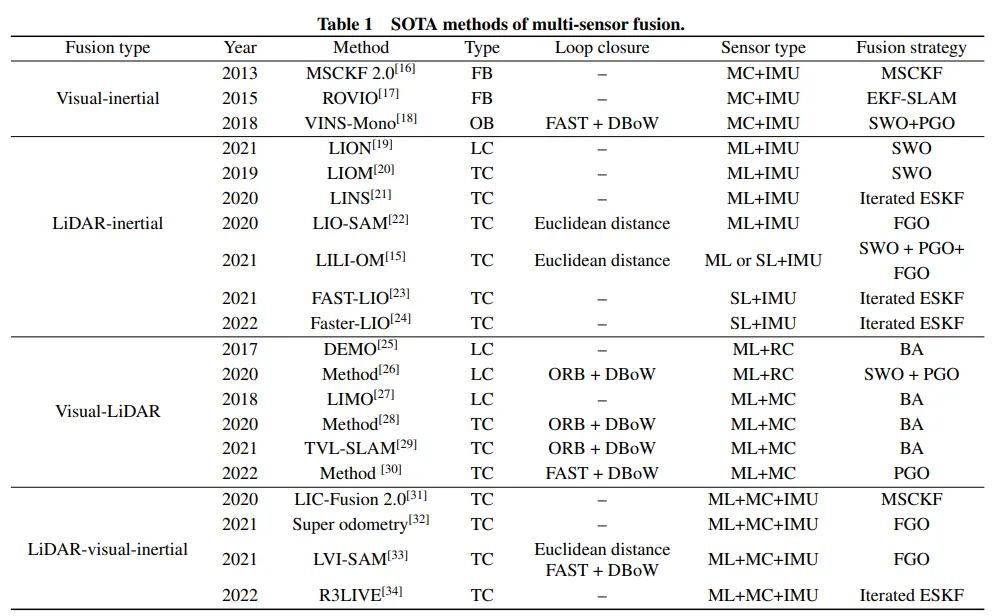
Original circuit
The following is the previous DI circuit shown in Figure 1:
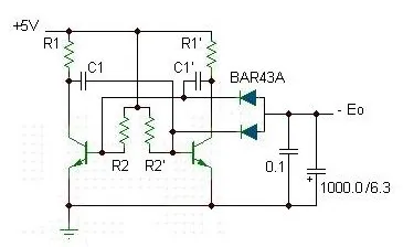
Figure 1 shows a simple local low-noise voltage converter, useful when a simple low-voltage negative supply is needed.
Modification using a potentiometer and an inductor
The circuit is simple and can be improved with a quick change to increase its efficiency. If R1 and R1' are fixed (keeping input power fixed), the output voltage reaches an extremum on Eo = Eo(R2). To facilitate reaching that extremum, the circuit from Figure 1 can be modified as shown in Figure 2, where a single potentiometer R2 adjusts the R2/R2' ratio.
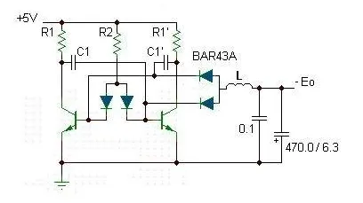
The main change is the addition of an inductor L at the output. A relatively low inductance, about 0.1 to 1.0 mH, is sufficient. This low value may conflict with a low-frequency multivibrator if its frequency is below 1 kHz.
Effects of the added inductor
The negative output voltage increases slowly with L: from -0.36 V at L = 0.1 mH to -0.4 V at L = 1 mH.
The primary benefit is that the output current (and effective voltage) increases by about 25%. The circuit in Figure 1 produced about -0.31 V, while the modified circuit in Figure 2 can provide over -0.39 V under the same 910 ohm load.
The inductor also significantly reduces output noise. With the same L, the output capacitor in Figure 2 can have roughly half the capacitance but the output noise amplitude is reduced by about half.
Suggested component values
Typical component values:
- L = 0.1 to 1.0 mH
- R1 = R1' = 5.6 kΩ
- R2 ≈ 22 kΩ
- C1 = C1' = 0.1 uF
The output capacitor should be low impedance.
The circuit draws less than 1.5 mA from a +5 V supply and produces more than -0.39 V into a 910 ohm load. An alternative circuit ("photocell enables op amp true-zero output") can provide the same output current but consumes roughly 10 times more power and exhibits about 100 times higher output noise.
Monitoring for voltage drops
These circuits can present a low voltage that may not directly affect the host system, but if that voltage drops the result can be distortion that is easy to overlook. To ensure detection of such voltage drops, use the circuit shown in Figure 3. It is useful for monitoring supply consistency in any dual-supply system.
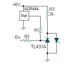
A green LED indicates "power good" and can serve as a system power-on indicator. Resistors R1 and R2 should be at least 1% tolerance. When the output voltage shift reaches e = -20 to -100 mV, the LED should illuminate depending on the buffer characteristics.
Design equations and example
For R1 and R2, define:
v1 = Vref + |e|
v2 = 2.5 + |e|
Then:
R1 = R2 * ((v1 / v2) - 1)
For a given reference and e = 50 mV:
R1 = 0.63 * R2
Example: R1 = 38.8 kΩ, R2 = 62 kΩ.
These values may require adjustment because the total resistance of the divider should not be too low; be cautious about the divider's output current. When the divider current is very low, the TL431 input current has a relatively large effect, so adjust accordingly. Any other reference with an output above 2.5 V can be used, but R1 and R2 must be recalculated for that reference.