 ALLPCB


Introduction
Signal integrity challenges arise as PCB designs push toward higher speeds and denser layouts, affecting data transmission quality across traces and vias. Engineers must address these issues early to prevent failures in performance, such as bit errors or timing violations. Effective management involves understanding fundamental principles and applying proven PCB design methods. This article explores signal integrity techniques, common pitfalls, and practical strategies for noise reduction in PCBs and interference reduction. By following structured approaches, designers can ensure reliable operation in demanding applications. Key to success lies in integrating these methods throughout the design process.
What Is Signal Integrity and Why It Matters in PCB Design
Signal integrity refers to the preservation of electrical signal quality from source to receiver, free from distortion or degradation. In PCB contexts, it encompasses factors like waveform shape, voltage levels, and timing accuracy. Poor signal integrity leads to issues such as increased jitter, eye closure, or complete signal loss, compromising system reliability. As clock rates exceed gigahertz ranges, even minor imperfections amplify into major problems. Industry standards like IPC-2221 provide guidelines for layout and spacing that support signal integrity from the outset. Mastering these concepts is essential for electric engineers tackling high-speed interfaces.
High-speed signals demand precise control over propagation characteristics to maintain data validity. Disruptions not only degrade performance but also increase electromagnetic emissions, complicating compliance efforts. Designers prioritizing signal integrity reduce debugging time and iteration costs during prototyping. Ultimately, robust signal integrity ensures products meet operational specs under real-world conditions, from consumer electronics to aerospace systems.
Common Causes of Signal Integrity Issues in PCBs
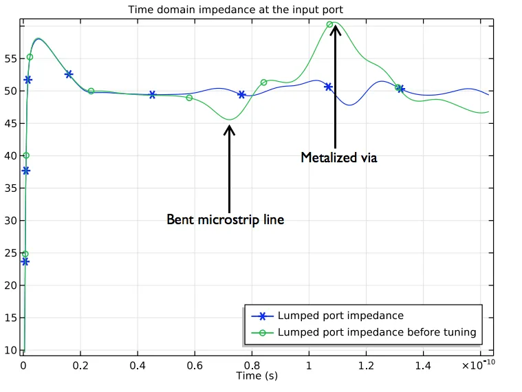
Reflections occur primarily from impedance discontinuities along transmission lines, such as unmatched trace widths or abrupt bends. These mismatches cause signal portions to bounce back, superimposing on the original waveform and distorting it. Vias, connectors, and component pads often introduce such discontinuities if not managed. Engineers observe these effects through ringing or overshoot in time-domain reflectometry measurements. Addressing reflection issues PCB starts with identifying these points during schematic review.
Crosstalk arises when electromagnetic coupling between adjacent traces induces unwanted voltage on victim lines. Aggressors switching rapidly generate near-end and far-end crosstalk, degrading noise margins. Factors like trace proximity, length overlap, and dielectric properties exacerbate this coupling. Ground bounce, another culprit, stems from simultaneous switching of multiple outputs sharing inductances in power/ground paths. These mechanisms collectively erode signal-to-noise ratios, demanding proactive PCB design methods.
Attenuation and dispersion further complicate matters as signals traverse longer paths or lossy materials. Higher frequencies suffer greater losses due to skin effect and dielectric absorption. Power supply noise couples into signals via inadequate decoupling or plane splits. Environmental factors like temperature variations can shift impedances, amplifying vulnerabilities. Understanding these causes forms the foundation for implementing effective signal integrity techniques.
PCB Design Methods for Impedance Control and Reflection Mitigation
Controlled impedance routing ensures traces maintain consistent characteristic impedance, minimizing reflections. Designers calculate stackup configurations to achieve target impedances using standard formulas accounting for trace width, thickness, and layer spacing. Symmetric stripline or microstrip geometries offer predictable performance. IPC-2221 outlines spacing and width guidelines that aid in this control. Terminations, such as series resistors or parallel capacitors, absorb reflected energy at line ends.
Length tuning equalizes propagation delays for parallel signals, preventing skew-induced errors. Serpentine or trombone patterns add delay without introducing excessive loss. Engineers verify compliance through pre-layout simulations modeling full channel paths. Avoiding vias in critical segments or using back-drilled vias reduces stub effects. These PCB design methods form core signal integrity techniques for multi-gigabit interfaces.
Proper via design transitions signals smoothly between layers, preserving integrity. Staggered or filled vias minimize inductance, while blind or buried types shorten paths. Transition zones with gradual width changes ease impedance steps. Post-layout extraction feeds these into verification tools for reflection analysis. Consistent application yields cleaner waveforms and wider eye openings.
Signal Integrity Techniques for Crosstalk and Noise Reduction in PCBs
Guard traces or stitching vias between aggressor and victim lines shield against capacitive and inductive coupling. Increasing separation distances follows exponential decay principles for field strength. Orthogonal routing on adjacent layers reduces broadside coupling. Ground planes adjacent to signal layers provide return paths, confining fields and lowering crosstalk. These interference reduction PCB strategies prove effective in dense layouts.
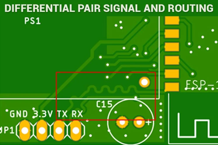
Differential signaling pairs convert common-mode noise to differential, enhancing rejection. Tight coupling and length matching within pairs boost common-mode impedance while minimizing loop areas. Engineers route pairs as symmetric twins, avoiding splits or crossings. This technique excels in USB or PCIe implementations. Combining with shielding planes achieves superior noise reduction in PCBs.
Decoupling capacitors placed near IC power pins shunt high-frequency noise, stabilizing supplies. Arrays of values target broad spectra, from bulk to high-frequency bypass. Solid power planes distribute current evenly, reducing droop. Via fencing around noisy sections isolates disturbances. These practices align with layered defense approaches for resilient designs.
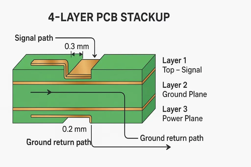
Layer Stackup and Routing Best Practices for Interference Reduction
Strategic layer assignment dedicates inner layers to signals flanked by planes, optimizing return paths. Signal-ground-signal stacking minimizes loop inductance for high-speed nets. Plane splits require careful bridging to avoid return current detours. Core and prepreg selection influences loss tangent, impacting attenuation. Simulations predict insertion loss across frequencies.
Routing high-speed nets first reserves optimal paths, avoiding congestion. 45-degree bends or curved traces reduce reflections over sharp 90-degree corners. Minimize vias by planning component placement thoughtfully. Groups of parallel buses benefit from broadside avoidance. These PCB design methods integrate seamlessly into workflows.
Power integrity ties closely to signal concerns, as PDN impedance affects noise injection. Low-ESR planes and dense decoupling form low-impedance paths up to GHz. Engineers model PDN resonance to place caps optimally. Avoiding clock lines near sensitive analog sections prevents injection. Holistic approaches yield interference reduction PCB success.
Troubleshooting Common Signal Integrity Problems
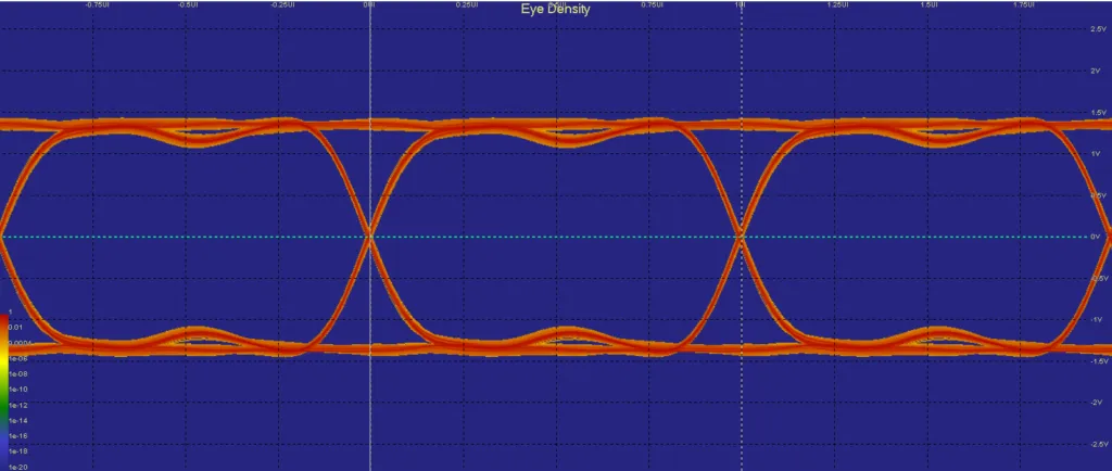
Engineers diagnose issues via oscilloscope eye patterns or TDR plots revealing reflections. Jitter decomposition isolates deterministic versus random sources. Crosstalk appears as glitches on quiet lines during aggressor transitions. Simulation-layout correlation refines models iteratively. Fabricating test coupons validates predictions.
Reflection issues PCB manifest as overshoot ringing; mitigation involves termination tweaks. Excessive crosstalk prompts spacing increases or shielding additions. Ground bounce shows voltage sags; more vias or planes resolve it. Iterative prototyping with measurements closes the loop. Documentation of fixes accelerates future designs.
Advanced cases employ field solvers for 3D extraction, capturing via fields accurately. Frequency-domain S-parameters quantify losses and coupling. Correlation with hardware builds confidence. Standards like IPC-6012E ensure fabricated boards meet performance specs. Systematic troubleshooting preserves project timelines.
Conclusion
Managing signal integrity demands a blend of foundational knowledge, disciplined PCB design methods, and verification rigor. From impedance control to routing finesse, each technique counters specific threats like reflections or crosstalk. Noise reduction in PCBs and interference reduction strategies elevate design margins. Electric engineers benefit from adhering to guidelines in IPC-2221 and similar standards. Proactive implementation minimizes risks, ensuring high-yield prototypes and reliable products. Continuous learning refines expertise in this evolving field.
FAQs
Q1: What are the primary signal integrity techniques for high-speed PCBs?
A1: Signal integrity techniques include controlled impedance routing, differential pairs, and adjacent ground planes to minimize reflections and crosstalk. Length matching prevents skew, while decoupling reduces supply noise. These PCB design methods ensure waveform fidelity across channels. Proper stackup planning further enhances performance by optimizing return paths.
Q2: How can engineers achieve noise reduction in PCBs effectively?
A2: Noise reduction in PCBs involves solid reference planes, strategic decoupling capacitor placement, and minimizing loop areas in routing. Shielding traces with guard lines or stitching vias isolates sensitive nets. Orthogonal layering cuts broadside coupling. These steps maintain clean signals amid dense integrations.
Q3: What PCB design methods address reflection issues PCB?
A3: Addressing reflection issues PCB requires impedance matching through consistent trace geometries and terminations at line ends. Avoid sharp bends and unnecessary vias to preserve continuity. Back-drilling eliminates stubs, while simulations predict mismatches. These methods deliver distortion-free propagation.
Q4: Why is layer stackup critical for interference reduction PCB?
A4: Layer stackup dictates field confinement and return path quality, key to interference reduction PCB. Signal layers between planes lower inductance and EMI. Material choices affect loss, influencing attenuation. Balanced configurations support multi-speed nets reliably.
References
IPC-2221B — Generic Standard on Printed Board Design. IPC, 2012
IPC-6012E — Qualification and Performance Specification for Rigid Printed Boards. IPC, 2017
J-STD-001H — Requirements for Soldered Electrical and Electronic Assemblies. IPC/JEDEC, 2018


