 ALLPCB


Introduction
Designing printed circuit boards (PCBs) for easy etching streamlines the manufacturing process and minimizes defects that can arise during chemical etching. PCB design for etching requires careful consideration of layout elements to accommodate the isotropic nature of the etching process, where copper removal occurs laterally as well as vertically. Engineers often overlook these aspects, leading to issues like undercutting, bridging, or uneven copper removal, which increase production costs and scrap rates. By following PCB layout tips tailored for etching, designers can achieve higher yields and faster turnaround times in fabrication. This article explores PCB manufacturing guidelines and design rules for PCB etching, providing structured engineering insights for electric engineers. Adopting these practices ensures reliable boards that meet performance expectations without compromising manufacturability.
What Is PCB Etching and Why Does Easy Etching PCB Design Matter?
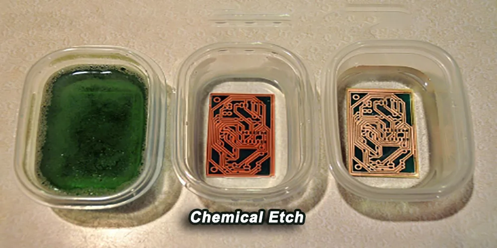
PCB etching involves selectively removing unwanted copper from laminated boards using chemical etchants, typically alkaline or acidic solutions, to form conductive traces, pads, and vias. This subtractive process defines the circuit pattern after imaging with photoresist. The relevance of easy etching PCB design lies in the etching's chemical aggression, which can erode resist edges and cause dimensional inaccuracies if the layout is not optimized. Poor designs lead to manufacturing rejects, as seen in over-etched traces or residual copper bridges that fail electrical testing. For electric engineers, prioritizing PCB design for etching integrates seamlessly with design for manufacturability (DFM), reducing iterations between design and production. Ultimately, these considerations enhance board reliability and support scalable production volumes.
Etching challenges stem from process variations, including etchant concentration, temperature control, and conveyor speed in panel processing. Designers must anticipate these to prevent yield losses that affect project timelines. IPC-2221 provides foundational guidelines for conductor dimensions and spacing to mitigate such risks. By aligning layouts with these standards early, engineers avoid costly revisions post-prototype.
Technical Principles of Etching in PCB Manufacturing
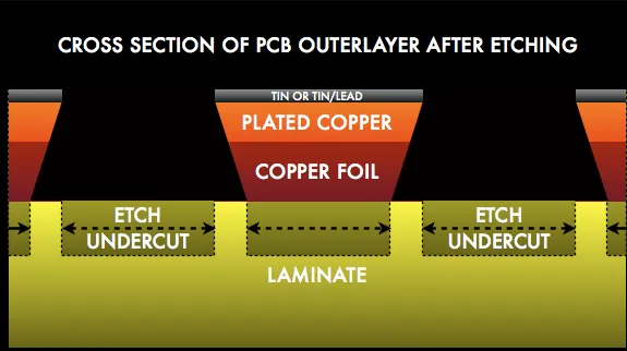
The core mechanism of PCB etching is isotropic dissolution of copper, meaning the etchant attacks equally in all directions, leading to undercutting beneath the photoresist mask. This undercut, often called the etch factor, typically results in traces narrowing by an amount proportional to copper thickness, demanding compensatory design adjustments. Sharp corners and acute angles exacerbate this, as etchant pools and accelerates removal at convex points, potentially creating pinholes or open circuits. Copper density variations across the panel cause uneven etching rates; high-density areas etch slower due to etchant depletion, while sparse regions over-etch.
These principles underscore the need for balanced copper distribution to maintain uniform etchant exposure. Panel-level effects, such as drag-out in conveyorized lines, further influence outcomes, making holistic layout planning essential. IPC-A-600 outlines acceptability criteria for etch-related defects like mouse bites or pitting, guiding designers toward robust features. Understanding these interactions allows engineers to predict and preempt fabrication issues systematically.
Surface preparation prior to etching, including micro-roughening, affects adhesion and uniformity but ties back to design through feature sizing. Vias and fine-pitch patterns amplify risks, as plating buildup alters etch dynamics on inner layers. Logical application of these principles in PCB layout tips ensures predictable results across production runs.
Best Practices and Design Rules for PCB Etching
Start with establishing minimum conductor widths and spacings that account for etching tolerances, as narrower features demand precise control prone to variation. IPC-2221 recommends scaling these based on copper weight and class of construction to prevent opens or shorts. Incorporate etch compensation by enlarging traces and pads laterally by an amount at least equal to the expected undercut, ensuring final dimensions meet functional needs after processing. This practice, integral to design rules for PCB etching, applies particularly to high-current paths where width accuracy is critical.
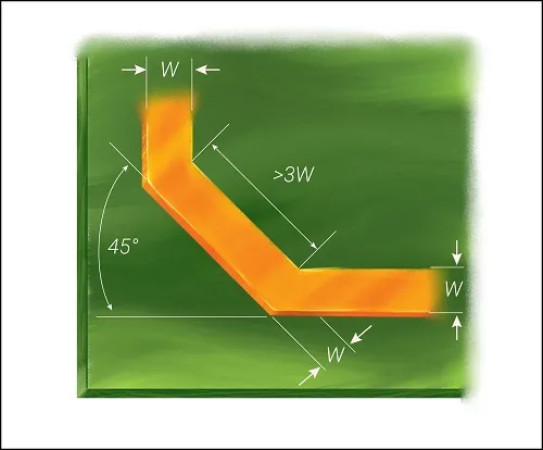
Favor 45-degree angles or smooth arcs over 90-degree corners in routing to distribute etchant flow evenly and reduce localized over-etching. Sharp turns create stress points where resist lifts or etches excessively, compromising integrity. Use teardrop transitions at pad-trace junctions to reinforce connections against etch-induced necks. These PCB layout tips promote smoother fabrication and align with manufacturing capabilities for fine-line boards.
Maintain copper balance across the panel, targeting uniform density between 40 and 60 percent to avoid differential etching rates that warp boards or leave residues. Group high-density features centrally and distribute ground planes thoughtfully, avoiding isolated islands. For multi-layer boards, balance each copper layer independently, as sequential etching processes compound imbalances. This guideline enhances overall panel yield and supports IPC-6012 performance specifications for rigid boards.
Optimize annular rings around vias and pads to at least the minimum required for plating and etching integrity, preventing ring breakout from undercut. Larger rings provide margin for drill wander and etch variance, especially in blind or buried vias. Tentable via sizes facilitate outer-layer protection during etching, reducing exposure risks. Panelization rules, such as V-scoring or tabbed arrays with fiducials, ensure stable handling without stressing etched edges.
Address inner-layer imaging by specifying sequential lamination processes compatible with etching sequences, minimizing alignment shifts from differential shrinkage. Avoid nested loops or interleaved patterns that trap etchant, leading to incomplete removal. Simulate etch profiles using design software rulesets to visualize potential defects early. These comprehensive PCB manufacturing guidelines integrate seamlessly into the design flow for electric engineers.
Common Pitfalls in PCB Design for Etching and Troubleshooting Insights
One frequent issue is ignoring fab-specific capabilities, resulting in designs beyond standard etching resolutions and causing widespread shorts or opens. Engineers should query manufacturer DFM feedback iteratively, adjusting spacings proactively. Another pitfall involves neglecting copper thickness scaling; thicker foils demand proportionally larger features and spacings to compensate for greater undercut volumes.
Overly ambitious fine-pitch routing without relief cuts leads to bridging, detectable via automated optical inspection post-etch. Troubleshooting involves reviewing artwork for violations and resimulating with adjusted etch factors. Warpage from unbalanced etching manifests in assembly failures, mitigated by symmetric layouts and frame rails. Case analyses reveal that adhering to IPC standards halves defect rates in high-volume runs.
Conclusion
Mastering PCB design for etching demands a structured approach rooted in etching physics and industry standards like IPC-2221 and IPC-A-600. Key practices include etch compensation, angle optimization, copper balancing, and robust annular rings, all enhancing manufacturability without sacrificing performance. Electric engineers benefit from these PCB layout tips by reducing prototypes, accelerating time-to-market, and ensuring reliable boards. Integrating design rules for PCB etching early fosters collaboration with fabrication teams, yielding cost-effective production. Prioritize these guidelines to transform challenging layouts into etch-friendly designs that perform consistently.
FAQs
Q1: What are the main PCB design for etching considerations for trace routing?
A1: In PCB design for etching, prioritize minimum widths and spacings per IPC-2221 to counter undercutting. Use 45-degree angles instead of sharp corners to prevent over-etching at bends. Apply etch compensation to traces and pads, scaling by copper thickness. Balance copper density across layers for uniform etchant attack. These steps ensure high yields in manufacturing.
Q2: How does copper balance affect easy etching PCB design?
A2: Copper balance in easy etching PCB design prevents uneven etching rates that cause residues or over-etching. Aim for 40-60 percent density per panel area to maintain consistent etchant flow. Distribute features symmetrically, avoiding dense clusters. This practice aligns with PCB manufacturing guidelines, reducing warpage and improving panel utilization. Review layers individually for multi-boards.
Q3: Why is etch compensation essential in design rules for PCB etching?
A3: Etch compensation in design rules for PCB etching offsets isotropic undercutting, preserving final trace widths. Scale features laterally by the etch factor, typically tied to foil thickness per IPC-2221. Without it, narrow paths risk opens post-processing. Pads and vias benefit similarly for plating integrity. Verify via design rule checks during layout.
Q4: What role do annular rings play in PCB layout tips for etching?
A4: Annular rings in PCB layout tips for etching provide margin against drill misalignment and undercut. Size them adequately to retain connection after processing, per acceptability standards. Larger rings suit high-reliability classes. This prevents breakout faults, especially in dense via fields. Balance with space constraints for optimal DFM.
References
IPC-2221B - Generic Standard on Printed Board Design. IPC, 2003
IPC-A-600K - Acceptability of Printed Boards. IPC, 2020
IPC-6012E - Qualification and Performance Specification for Rigid Printed Boards. IPC, 2017





