ALLPCB


Semiconductor advances are driving the rise of artificial intelligence. In 1997, IBM's Deep Blue supercomputer defeated world chess champion Garry Kasparov. That demonstration highlighted breakthroughs in high-performance computing and suggested that computing might one day surpass human levels of intelligence. Over the following decade, AI began to be applied to many practical tasks such as facial recognition, language translation, and recommending movies and products.
Fifteen years later, AI has progressed to the point of synthesizing knowledge. Generative models like ChatGPT and Stable Diffusion can compose poetry, create artwork, assist in medical diagnosis, produce summaries and computer code, and even design integrated circuits comparable to human designs.
AI has become a digital assistant across many fields. ChatGPT illustrates how AI can democratize access to high-performance computing and provide practical benefits across society.
These AI advances rest on three factors: innovations in efficient machine learning algorithms, availability of massive datasets for training neural networks, and energy-efficient computing enabled by semiconductor technology. Although ubiquitous, the last factor often receives less attention than it deserves.
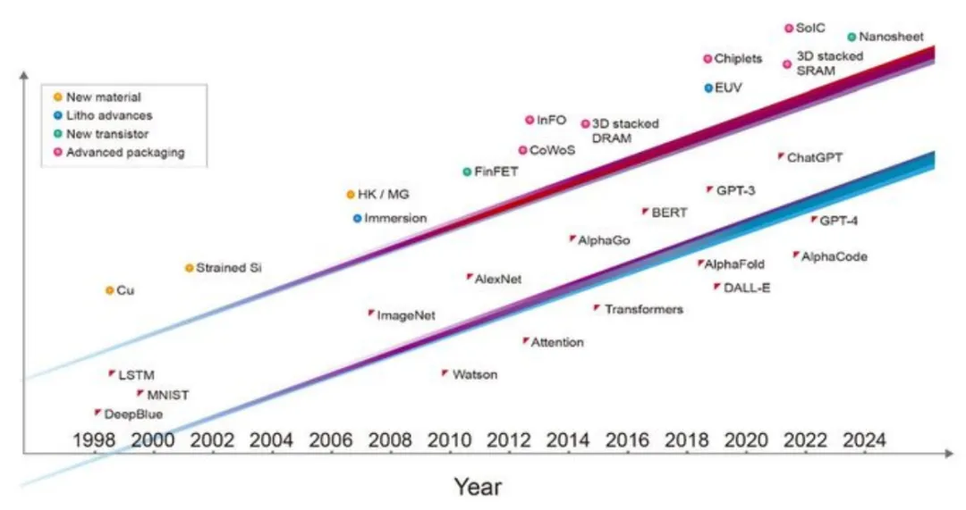
Over the past thirty years, major AI milestones depended on the leading semiconductor technology of their time. Deep Blue used a mix of 0.6 and 0.35 micron process technology. The deep neural networks that won ImageNet and launched the current era of machine learning were built on 40 nm technology. AlphaGo used 28 nm, and the initial ChatGPT training ran on servers built with 5 nm technology. Later versions of ChatGPT have been supported by servers using more advanced 4 nm process nodes. Every layer of the computing stack, from software and algorithms to architecture, circuit design, and device technology, acts as a multiplier for AI performance. It is fair to say that fundamental transistor technology has driven progress across those layers.
If the AI revolution is to continue at its current pace, the semiconductor industry will need to contribute further. Within a decade, AI workloads will demand a GPU with one trillion transistors, roughly ten times the device count of typical devices today.
Growing Compute and Memory Demands
Compute and memory access requirements for AI training have increased by orders of magnitude in the past five years. For example, training GPT-3 required the equivalent of over 5 billion operations per second sustained for an entire day (5,000 petaflop-days) and about 3 trillion bytes (3 TB) of memory capacity.
New generative AI applications continue to drive rapid growth in both compute and memory needs. The critical question is: how can semiconductor technology keep pace?
From Integrated Devices to Integrated Multi-Chip Systems
Since the invention of the integrated circuit, semiconductor progress focused on shrinking feature sizes to pack more transistors onto a chip. Today integration has moved to a higher level: beyond 2D scaling into 3D system integration. Many chips are being combined into tightly integrated, large-scale interconnected systems. This represents a paradigm shift in semiconductor integration.
In the AI era, system capability scales with the number of transistors integrated into the system. A primary limit is that lithography tools are designed to fabricate individual ICs up to roughly 800 mm2, the so-called reticle size limit. However, system size can now be extended beyond the reticle limit by connecting multiple chips to a larger interposer layer, a silicon piece with built-in interconnects. For example, TSMC's CoWoS wafer-level packaging can host up to six reticle-area compute dies plus more than a dozen high-bandwidth memory (HBM) stacks.
How Nvidia Uses CoWoS Advanced Packaging
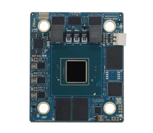
CoWoS is TSMC's advanced package-on-wafer technology, and it is used in commercial products. Examples include Nvidia's Ampere and Hopper GPUs. Each package combines a GPU die and six HBM cubes, all mounted on a silicon interposer. The compute GPU die area is approximately the maximum allowed by current lithography tools. Ampere has about 54 billion transistors and Hopper about 80 billion. The shift from 7 nm to denser 4 nm technology increased transistor count in the same area by about 50 percent. Ampere and Hopper are widely used to train large language models. Training large-scale models requires tens of thousands of such processors.
HBM exemplifies another critical semiconductor technology for AI: integrating chips by stacking them vertically. HBM consists of stacked DRAM chips above control logic die, using through-silicon vias (TSVs) for vertical interconnects and solder bumps to form connections between memory chips. High-performance GPUs commonly use HBM today.
Looking ahead, 3D SoIC technologies can offer an alternative to conventional HBM by providing denser vertical interconnects between stacked chips without solder bumps. Recent progress shows test structures with 12-layer stacks using hybrid bonding, where copper-to-copper connections achieve higher density than solder bumps. Those memory stacks can be bonded at low temperature onto larger base logic dies with total thicknesses around 600 μm.
For high-performance systems composed of many chips running large AI models, wired electrical links may soon limit compute speed. Optical interconnects are already used to connect server racks in data centers. The next step will be silicon photonics optical interfaces integrated with GPU and CPU packages. That will allow scalable, energy- and area-efficient bandwidth for direct optical GPU-to-GPU communication, enabling hundreds of servers to act as a single giant GPU with shared memory. Silicon photonics will become one of the most important enabler technologies for the semiconductor industry due to AI demands.
Toward Trillion-Transistor GPUs
How AMD Uses 3D Technologies
AMD's MI300A accelerator uses not only CoWoS but also TSMC's 3D SoIC technologies. MI300A combines GPU and CPU cores designed for large AI workloads. The GPU executes dense matrix operations for AI, the CPU manages computation, and high-bandwidth memory (HBM) serves both. Nine compute dies built on 5 nm are stacked over four 6 nm base dies that handle caching and I/O traffic. The base dies and HBM sit on a silicon interposer. The processor's compute portion contains about 150 billion transistors.
As noted, typical AI training GPU chips have already reached the reticle-area limit. Their transistor counts are on the order of 100 billion. Continued growth in transistor count will require multiple dies interconnected via 2.5D or 3D integration to perform computation. Integrating multiple dies with CoWoS, SoIC, and related advanced packaging can yield a system transistor count far exceeding what can be placed on a single die. We project that within a decade, multi-die GPUs will exceed one trillion transistors.
All these small dies must be connected in 3D stacks, but industry progress has rapidly decreased vertical interconnect pitch to increase connection density. There appears to be room for further improvement. Interconnect density could reasonably grow by an order of magnitude or more.
Energy-Efficient Performance Trends for GPUs
How will these hardware innovations improve system performance?
One observable trend is steady improvement in a metric called energy-efficient performance, or EEP. EEP combines system energy efficiency and speed. Over the past 15 years, semiconductor energy efficiency for this metric has improved roughly threefold every two years. We expect this trend to continue, driven by innovations across materials, devices, integration, extreme ultraviolet (EUV) lithography, circuit design, system architecture, and joint optimization of these elements.
Overall, EEP is expected to double approximately every two years, measured in units of 1/fJ·ps. In particular, increases in EEP will be enabled by the advanced packaging techniques discussed here. Concepts such as system technology co-optimization (STCO) will become increasingly important, where different functional parts of a GPU are separated into smaller dies and each part is built using the most appropriate and cost-effective process technology.
The Mead-Conway Moment for 3D Integration
In 1978, Caltech professor Carver Mead and Lynn Conway at Xerox PARC developed computer-aided design methods for integrated circuits. They used a set of design rules to describe chip scaling so engineers could design very-large-scale integrated (VLSI) circuits without deep process knowledge.
3D chip design needs the same capability today. Designers must understand chip design, system architecture, and hardware-software co-optimization. Manufacturers must understand process technology, 3D IC techniques, and advanced packaging. As in 1978, a common language is needed that electronic design tools can use to describe these technologies. Such a hardware description approach lets designers create 3D IC systems without focusing on low-level process details. That standard is emerging: an open standard called 3Dblox has been accepted by most major technology and EDA companies.
Beyond the Tunnel
In the AI era, semiconductor technology is the key driver for new AI capabilities and applications. New GPUs are no longer constrained by historical chip size and form factors. New semiconductor advances go beyond shrinking transistors in a 2D plane. Integrated AI systems will be composed of as many energy-efficient transistors as needed, efficient system architectures tailored for specific workloads, and tight optimization between software and hardware.
For the past 50 years, semiconductor progress resembled traveling through a tunnel: the path forward was clear because the next step—smaller transistors—was well defined. Now we have reached the tunnel's end. From here, semiconductor progress will be harder to chart. Yet beyond the tunnel lie many new possibilities.