 ALLPCB


Introduction
Sequential build-up PCBs represent a cornerstone in modern high-density interconnect technology, enabling compact designs for advanced electronics. These boards undergo a layer-by-layer construction process that integrates fine-line features and microvias, crucial for high-speed signal integrity and miniaturization. As electric engineers push the boundaries of performance in applications like telecommunications and computing, adhering to sequential build-up PCB design rules becomes essential to avoid manufacturing defects and ensure long-term reliability. Poorly planned stackups or via configurations can lead to issues such as warpage, delamination, or electrical shorts, amplifying costs during production. This article outlines key sequential build-up PCB manufacturing guidelines and DFM considerations, providing structured insights for robust outcomes. By following these sequential build-up PCB best practices, engineers can optimize yield and functionality.
What Is Sequential Build-Up PCB and Why It Matters
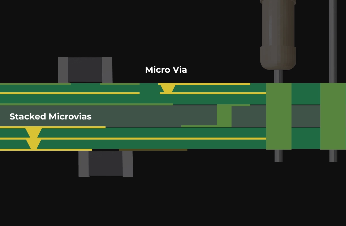
Sequential build-up, often abbreviated as SBU, involves iteratively applying dielectric materials and copper layers on a core substrate, followed by precise via formation through laser drilling or plasma etching. Unlike traditional multilayer PCBs built in a single lamination cycle, SBU allows for controlled buildup of additional layers, supporting microvia densities that exceed standard capabilities. This process facilitates stacked or staggered vias, enabling shorter interconnect paths and reduced signal loss in high-frequency designs. For electric engineers, SBU PCBs are vital in scenarios demanding high I/O counts, such as server motherboards or RF modules, where conventional methods fall short.
The relevance of sequential build-up PCB design rules stems from the process's inherent complexities, including multiple plating cycles and material interactions that heighten risks of misalignment or thermal stress. Manufacturing yields can drop significantly without proper DFM, leading to scrap rates that impact project timelines and budgets. Robust SBU designs ensure compliance with performance specifications, maintaining signal integrity up to multi-GHz frequencies. Moreover, as device densities increase, these guidelines prevent field failures from via cracking or interlayer shorts, safeguarding product reputation.
Core Technical Principles of Sequential Build-Up PCBs
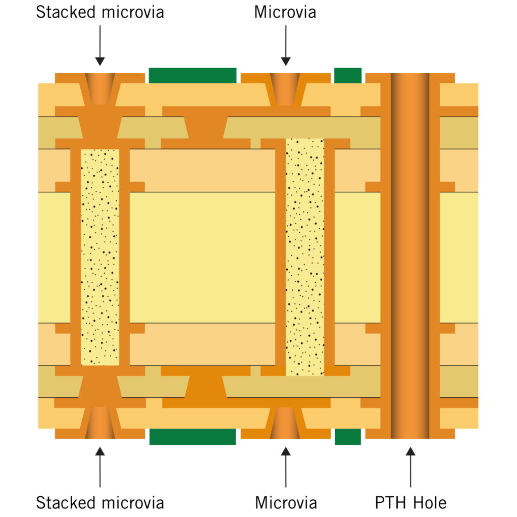
At the heart of SBU lies the stackup architecture, typically classified as 1+N+1 or 2+N+2 configurations, where N denotes buildup layers on both sides of a central core. Each buildup cycle adds a photosensitive dielectric resin, followed by copper deposition via electroless plating and electroplating, with vias formed to connect sequential layers. Laser ablation creates blind or through vias with diameters as small as 50 microns, demanding precise control over beam focus and energy to avoid resin smear or fiber damage in glass-reinforced dielectrics. The aspect ratio of these vias, defined as depth to diameter, influences plating uniformity and reliability under thermal cycling.
Material selection plays a pivotal role, with low-coefficient of thermal expansion (CTE) resins matching copper's properties to mitigate warpage during reflow soldering. Buildup foils must exhibit uniform thickness and adhesion strength, as variations can cause registration errors in subsequent imaging steps. Sequential build-up PCB manufacturing guidelines emphasize symmetric stackups to balance mechanical stresses, preventing bow and twist that exceed allowable limits. Electrical testing at each buildup stage verifies continuity and insulation resistance, ensuring no latent defects propagate.
Thermal management principles guide copper weight distribution, with outer layers often thinner to accommodate fine lines while inner layers handle power distribution. Plating thickness uniformity, targeted at 15-20 microns per cycle, supports current carrying capacity without excessive buildup that could stress dielectrics. These mechanisms collectively enable SBU PCBs to achieve routing densities over 100,000 nets per square decimeter, far surpassing standard multilayers.
Essential Sequential Build-Up PCB Design Rules
Engineers must prioritize via design rules to ensure robust sequential build-up PCB DFM. Microvias should maintain an aspect ratio not exceeding 1:1 for reliable plating void-free fill, preventing electromigration under high currents. Stacked vias require intermediate annular ring support from underlying copper pads, with overlap dimensions scaled to drill tolerances. Filled vias, using conductive or non-conductive pastes, enhance planarization for subsequent layers, but demand bake cycles to expel volatiles and avoid popcorn cracking.
Line and space widths narrow progressively in outer buildup layers, starting at 50/50 microns for signal traces and widening for power planes. Sequential build-up PCB design rules dictate minimum clearances between features to prevent bridging during patterning, typically 75 microns for high-density regions. Panelization strategies influence yield, with array sizes limited to 18x24 inches to control warpage during lamination presses. Edge beveling and fiducial marks aid alignment, compensating for material shrinkage up to 0.5% per axis.
Stackup symmetry forms a foundational sequential build-up PCB best practice, mirroring buildup thicknesses on both core sides to neutralize residual stresses from curing. Core thickness selection balances rigidity against total board thinness, often 0.8mm for high-layer counts. Material CTE mismatch below 20 ppm/°C between dielectric and copper minimizes via barrel cracking, as outlined in IPC-6012E qualification specs for rigid printed boards. Registration budgets allocate tolerances across drilling, imaging, and etching, ensuring via-to-pad capture exceeds 50% land area.
Sequential Build-Up PCB Manufacturing Guidelines and DFM Best Practices
DFM begins with artwork scaling to account for dielectric shrinkage, applying factors derived from material datasheets. Sequential build-up PCB manufacturing guidelines recommend sequential lamination with vacuum pressing to achieve void-free bonds, reducing moisture absorption risks per JEDEC J-STD-020E moisture sensitivity classifications. Plasma cleaning precedes buildup to enhance adhesion, removing residues that could cause peel-offs. Plating bath chemistry must maintain additive concentrations for uniform deposition, avoiding dog-boning at via entrances.
Warpage control integrates mechanical fixtures during processing, with final bow and twist held below 0.75% for boards under 16 inches. Sequential build-up PCB DFM stresses tear-drop pad shapes at vias to distribute stresses and improve etch yields. Impedance control for high-speed traces requires stackup modeling, targeting 50 ohms single-ended with dielectric constants verified post-buildup. Final fabrication includes flying probe testing for opens/shorts, followed by cross-section analysis for via quality.
Best practices extend to handling, mandating bake-outs at 125°C for 24 hours to desorb moisture before laser drilling. Sequential build-up PCB best practices include specifying buildup sequence in fab drawings, clarifying core versus buildup layers. These guidelines, when integrated early, elevate first-pass yields above 90% in production runs.
Common Challenges and Troubleshooting Insights
Warpage emerges as a frequent issue in asymmetric stackups, exacerbated by core-to-buildup thickness disparities. Troubleshooting involves iterative FEA simulations to predict deformations, adjusting copper balances accordingly. Via fill inconsistencies signal plating issues, resolved by current density profiling and dummy plating cells. Delamination at interfaces traces to poor surface preparation, addressed via desmear optimization using permanganate etches.
Registration drift accumulates across cycles, mitigated by optical alignment systems and multi-fiducial grids. Sequential build-up PCB design rules counter these by conservative aspect ratios and enlarged capture pads. Electrical opens post-plating often stem from smear residue, preventable through optimized laser parameters and post-drill etches.
Conclusion
Mastering sequential build-up PCB design rules unlocks reliable high-density boards for demanding applications. From symmetric stackups and via aspect ratios to DFM-driven manufacturing guidelines, these practices ensure mechanical integrity and electrical performance. Electric engineers benefit from proactive adherence, minimizing iterations and enhancing product lifecycles. Integrating sequential build-up PCB best practices aligns designs with fabrication realities, fostering innovation without compromise.
FAQs
Q1: What are the key sequential build-up PCB design rules for via reliability?
A1: Via aspect ratios should stay below 1:1 to ensure plating uniformity, with stacked configurations using adequate annular ring overlaps. Filled vias require post-fill bakes to prevent voids. These rules, per standard qualifications, reduce cracking risks under thermal stress. Proper pad sizing captures drill tolerances effectively.
Q2: How do sequential build-up PCB manufacturing guidelines address warpage?
A2: Symmetric stackups balance CTE stresses, while vacuum lamination minimizes voids. Panels stay within size limits, and fixtures control bow during cooling. Final specs hold twist below 0.75%, supporting assembly yields. Moisture control per JEDEC standards prevents exacerbations.
Q3: Why is stackup symmetry a core sequential build-up PCB DFM practice?
A3: It neutralizes residual curing stresses, avoiding delamination or via failures. Matching buildup on both core sides maintains flatness for fine-pitch assembly. Engineers model imbalances early to adjust copper distributions. This best practice boosts overall reliability.
Q4: What sequential build-up PCB best practices improve high-speed signal integrity?
A4: Impedance-controlled traces with verified dielectrics reduce losses. Staggered vias shorten paths, minimizing crosstalk. Sequential build-up PCB design rules enforce line/space minima for routing density. Post-fab verification confirms performance margins.
References
IPC-6012E — Qualification and Performance Specification for Rigid Printed Boards. IPC, 2017
JEDEC J-STD-020E — Moisture/Reflow Sensitivity Classification. JEDEC, 2014
IPC-A-600K — Acceptability of Printed Boards. IPC, 2020


