 ALLPCB


Introduction
Double-sided PCB silkscreen plays a critical role in modern electronics by providing component identification, polarity markers, and assembly instructions on both surfaces of a board. Engineers working on advanced PCB design often encounter alignment issues that affect readability and manufacturing yield. These challenges become more pronounced in multi-layer PCB silkscreen applications where precise registration between top and bottom layers is essential. Proper management of silkscreen alignment on both sides helps maintain functional clarity throughout the product lifecycle. Addressing these dilemmas early in the design phase supports reliable production outcomes.
What Is Double-Sided Silkscreen and Why It Matters
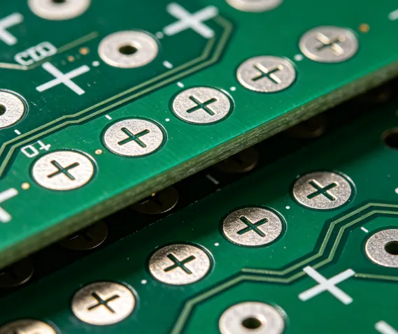
Double-sided PCB silkscreen refers to the application of ink-based legends on both the top and bottom surfaces of a printed circuit board. This technique supplies essential information such as part numbers, orientation indicators, and test points that guide assembly and maintenance teams. In multi-layer PCB silkscreen workflows, the process requires careful coordination to ensure legends remain legible after lamination and etching steps. Silkscreen registration accuracy directly influences inspection efficiency and reduces the risk of assembly errors. Industry professionals recognize that consistent alignment supports traceability requirements in complex electronic systems.
Technical Principles and Mechanisms of Alignment Challenges
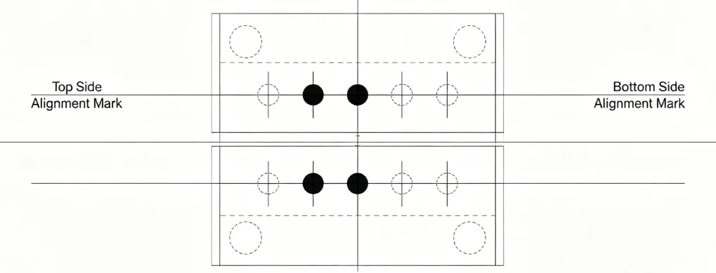
Alignment difficulties in double-sided PCB silkscreen stem from cumulative tolerances introduced during imaging, exposure, and curing stages. Board material expansion or contraction under thermal stress can shift the relative positions of top and bottom legends. In advanced PCB design, fiducial marks and registration holes serve as reference points, yet deviations still occur when layer-to-layer stacking tolerances exceed acceptable limits. Engineers analyze these mechanisms through coordinate measurement systems that compare actual legend positions against design data. Understanding the interaction between substrate properties and process parameters allows for targeted adjustments that improve overall registration precision.
Causes of Silkscreen Misregistration in Multi-Layer Boards
Several factors contribute to silkscreen misalignment on both sides of a board. Differential shrinkage between copper layers and dielectric materials during curing creates mechanical stresses that displace ink patterns. Equipment calibration drift in screen printing or inkjet systems further compounds these issues, particularly when boards undergo multiple thermal cycles. In multi-layer PCB silkscreen production, accumulated tolerances from prior lamination steps reduce the margin for accurate legend placement. Systematic root-cause analysis helps isolate whether the primary driver is material behavior or process variation.
Related Reading: The High Cost of Offset Silkscreen: Preventing Misalignment in PCB Manufacturing
Practical Solutions and Best Practices for Improved Registration
Designers mitigate alignment challenges by incorporating oversized fiducials and redundant registration features that accommodate expected variations. Specifying tighter process controls during artwork generation ensures that silkscreen data files maintain consistent scaling relative to copper layers. In advanced PCB design reviews, simulation of thermal expansion effects guides the selection of appropriate ink types and curing profiles. Collaboration between design and manufacturing teams verifies that proposed solutions remain compatible with existing equipment capabilities. These measures collectively enhance silkscreen registration without introducing unnecessary complexity.
Related Reading: PCB Silkscreen Design: Legibility and Industry Standards
Quality Control Approaches Aligned with Industry Standards
Quality verification of double-sided PCB silkscreen follows established inspection criteria that quantify acceptable deviation limits. Visual and optical measurement techniques confirm that legends maintain required clearance from conductors and pads. When deviations approach tolerance boundaries, corrective actions such as artwork revision or process recalibration restore compliance. These practices draw on principles outlined in IPC-A-600 to ensure consistent acceptance across production batches.
Troubleshooting Insights for Persistent Alignment Issues
When silkscreen registration problems persist, engineers examine panel-level warpage measurements taken before and after legend application. Adjustments to support fixtures during printing can reduce flexure that contributes to positional drift. In some cases, switching to a lower-temperature curing ink improves dimensional stability across both board surfaces. Documenting each iteration of the troubleshooting process builds a knowledge base that accelerates resolution in subsequent designs. This structured approach minimizes downtime and maintains production schedules.
Conclusion
Effective management of double-sided PCB silkscreen alignment requires attention to material behavior, process controls, and design practices. By applying logical evaluation methods, engineers achieve reliable registration that supports both assembly accuracy and long-term product serviceability. Consistent application of these principles reduces rework and strengthens overall manufacturing outcomes in advanced PCB design projects.
FAQs
Q1: What are the main causes of misalignment in double-sided PCB silkscreen?
A1: Misalignment typically arises from thermal expansion differences in substrate materials and cumulative tolerances during imaging and curing. Engineers evaluate these factors through coordinate measurements to identify whether material properties or equipment settings require adjustment. Systematic analysis helps isolate the dominant contributor and guides corrective actions that restore registration accuracy.
Q2: How does silkscreen registration affect multi-layer PCB silkscreen production?
A2: Accurate registration ensures that legends on both sides remain properly positioned relative to underlying copper features. Poor alignment can obscure component markings or violate clearance requirements, complicating assembly and inspection. Maintaining tight control over registration supports traceability and reduces the likelihood of functional errors in finished assemblies.
Q3: What design practices improve silkscreen alignment on both sides?
A3: Incorporating oversized fiducials and accounting for expected material expansion during artwork creation helps accommodate process variations. Designers also review layer stack-up data to verify scaling consistency between copper and silkscreen layers. These steps enhance registration reliability without adding excessive cost or complexity.
Q4: Why is silkscreen registration important in advanced PCB design?
A4: Precise registration guarantees that identification and orientation information remains legible after all manufacturing steps. This clarity aids assembly teams and field service personnel while meeting traceability expectations. Proper attention to registration therefore contributes to higher yield and lower defect rates throughout the product lifecycle.
References
IPC-A-600K — Acceptability of Printed Boards. IPC, 2020
IPC-6012E — Qualification and Performance Specification for Rigid Printed Boards. IPC, 2017


