 ALLPCB


Introduction
Electronics hobbyists often dive into building circuits with enthusiasm, but safety remains a top priority, especially when dealing with higher voltages. Creepage distance plays a crucial role in preventing electrical hazards like arcing or short circuits on printed circuit boards (PCBs). Understanding creepage distance basics helps you design reliable projects that keep you safe while experimenting. This guide breaks down what is creepage distance, why it matters for your workbench, and practical tips to apply it. By the end, you will feel confident incorporating electronic safety for hobbyists into your designs. Let's explore this essential concept step by step.
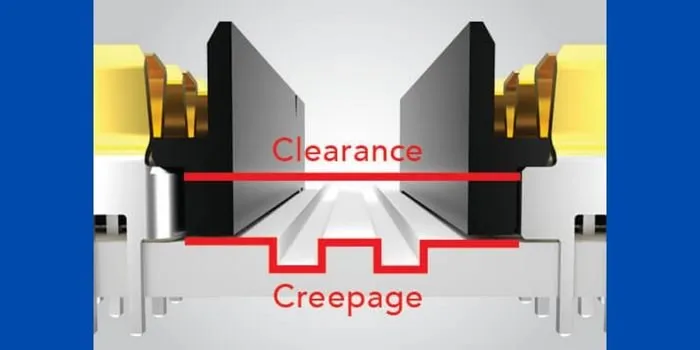
What Is Creepage Distance? Why It Matters for Hobbyists
Creepage distance refers to the shortest path along the surface of an insulating material, such as a PCB substrate, between two conductive parts like traces or pads. Unlike clearance, which measures the straight-line distance through air, creepage follows the contours of the board's surface. This distinction becomes critical in electronics where surface contamination or moisture can create conductive paths. For hobbyists building power supplies or sensor boards, ignoring creepage distance explained here can lead to failures or shocks. Proper creepage ensures insulation withstands voltage stress over time.
In everyday projects, creepage protects against flashover, where electricity jumps across the surface under high voltage. Hobbyists working with mains-powered devices or battery boosters face real risks if traces are too close. Standards like IPC-2221 provide guidelines for these spacings based on voltage levels and environments. This makes creepage distance basics a foundational part of electronic safety for hobbyists. Mastering it elevates your projects from functional to robust.
Why does it matter? Poor creepage design causes intermittent faults, overheating, or fires in worst cases. Hobby spaces often have dust or humidity, mimicking pollution degrees in industrial settings. By prioritizing creepage, you extend board life and focus on creativity rather than troubleshooting disasters. Simple awareness turns potential pitfalls into strengths.
The Technical Principles Behind Creepage Distance
Creepage distance arises from the need to prevent surface tracking, where voltage gradually degrades insulation along the path. Conductive particles, moisture, or residues lower the surface's resistance, allowing current to creep between conductors. Higher voltages demand longer paths to distribute electric field stress evenly. Factors like material's comparative tracking index (CTI) influence minimum distances, as higher CTI materials resist tracking better. Hobbyists select FR-4 PCBs, common for their balance of cost and performance.
Pollution degree classifies environments: degree 1 for clean sealed units, up to degree 4 for outdoor exposure. Your garage bench likely falls between degrees 2 and 3, requiring conservative spacings. Overvoltage categories, from category I for electronics to IV for utility lines, further adjust requirements. IEC 60664-1 outlines these principles for low-voltage insulation coordination. Understanding these helps hobbyists scale designs safely.
The path measurement starts from the edge of one conductor, follows any contours or barriers, and ends at the other. Slots or grooves in the PCB can extend effective creepage by forcing a longer route. Conformal coatings add a protective layer, effectively increasing distance by encapsulating the surface. These mechanisms ensure reliability without oversized boards.
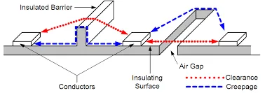
Factors Affecting Creepage Distance in Your Projects
Voltage rating stands as the primary driver for creepage requirements. Working voltage, the highest continuous RMS or DC value, dictates the baseline distance. Impulse voltages from transients demand even more margin. Hobbyists using 5V to 48V DC see modest needs, but AC adapters push toward stricter rules. Always consider peak voltages for safety.
Material properties matter too. PCB laminates with high CTI, grouped into classes I to IIIb per standards, allow shorter creepages. Most hobby FR-4 falls in group IIIa or IIIb, suitable for moderate voltages. Surface finish, like solder mask, influences tracking resistance. Test your setup's cleanliness to gauge real-world pollution.
Environmental factors amplify needs. Humidity absorbs into surfaces, reducing insulation strength. Dust from soldering settles on boards, creating bridges. Temperature swings expand materials differently, stressing paths. Hobbyists mitigate with enclosures or coatings for consistent performance.
Board geometry offers solutions. Wider traces reduce field concentration, but spacing rules dominate. Vias and components complicate paths, requiring checks around pins. Design software flags violations, easing verification.
Practical Best Practices for Implementing Creepage Distance
Start with conservative spacings in your PCB layout software, exceeding minimums for hobby margins. Route high-voltage traces on opposite layers, using vias sparingly. Separate power and ground planes where possible to maximize isolation. This approach simplifies creepage distance explained in designs.
Incorporate slots or trenches between critical sections. A milled groove doubles effective distance without extra board size. For dense boards, angle traces to lengthen surface paths naturally. Verify with design rule checks before fabrication.
Apply conformal coating post-assembly. Thin acrylic or silicone layers boost creepage by 2-3 times in polluted environments. Cure properly to avoid bubbles that create weak spots. Hobbyists brush or spray in ventilated areas for even coverage.
Test prototypes rigorously. Use a high-voltage tester at 1.5 times working voltage, ramping slowly. Inspect under magnification for defects. Iterate if arcing occurs.
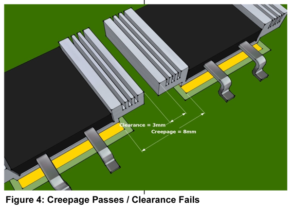
Troubleshooting Common Creepage Issues in Hobbyist Builds
Hobby projects often reveal creepage problems during testing. Arcing sparks indicate insufficient distance; measure paths and adjust. Intermittent shorts point to contamination; clean with isopropyl alcohol and retest.
Flashover leaves carbon tracks on surfaces. Polish gently and recoat. Component leads too close? Reposition or add standoffs. These fixes restore safety quickly.
Overheating near junctions suggests field crowding. Widen clearances there first. Humidity failures? Seal with potting compound. Systematic checks build intuition.
A simple case: a 24V motor driver PCB failed outdoors. Short creepage across solder mask allowed moisture bridging. Adding slots and coating resolved it, preventing repeats. Such insights apply broadly.
Conclusion
Creepage distance demystified reveals its role as a safety cornerstone for electronics hobbyists. From definitions to practices, prioritizing it ensures projects withstand real-world stresses. Reference standards like IPC-2221 for guidance, adapting to your voltage and environment. Integrate these basics into workflows for reliable, shock-free builds. Experiment confidently, knowing electronic safety for hobbyists starts with surface paths. Your next board will thank you.
FAQs
Q1: What is creepage distance in simple terms?
A1: Creepage distance is the shortest path along a PCB's insulating surface between two conductors, and it helps prevent surface arcing. It differs from clearance, which is the straight-line distance through air. For hobbyists, maintaining proper creepage distance avoids shocks and improves reliability as voltages increase.
Q2: Why is creepage distance vital for electronic safety for hobbyists?
A2: Creepage resists flashover caused by dust, moisture, and voltage stress on PCB surfaces. Hobby environments often mimic polluted conditions, so spacing per standards like IPC-2221 protects users and components while extending board life. Verifying creepage during prototyping ensures confidence before deployment.
Q3: How do I calculate creepage distance for my PCB project?
A3: Determine working voltage, pollution degree, and material CTI first. Consult minimum creepage tables in IEC 60664-1 and then add design margin. EDA tools can automate rule checks during routing. As a conservative hobby approach, start with distances about twice the minimum and refine after testing.
Q4: Can conformal coating improve creepage distance for hobbyists?
A4: Yes. Conformal coatings encapsulate the surface, increasing effective creepage and resisting contamination. Choose a coating suitable for your environment (e.g., acrylic for indoor use), apply evenly after soldering, and test to confirm the improvement.
References
IPC-2221B — Generic Standard on Printed Board Design. IPC, 2003
IEC 60664-1 — Insulation Coordination for Equipment within Low-Voltage Systems. IEC, 2007
IPC-9592B — Requirements for Power Converter Design. IPC, 2012
Texas Instruments — Creepage and Clearance (SLUP419)
EMA-EDA — PCB Clearance and Creepage Distance Table:





