 ALLPCB


In the fast-evolving world of electronics, high-density PCBs (Printed Circuit Boards) are at the heart of cutting-edge devices, from smartphones to medical equipment. A critical factor in their performance and reliability is the quality of solder joint formation. If you're facing challenges with solder joint formation in high-density PCB assembly, particularly with fine-pitch components or high-density interconnect (HDI) designs, this guide is for you. We'll dive deep into the hurdles, solutions, and best practices to ensure robust connections, covering topics like solder paste selection for HDI and reflow profiling for high-density interconnect.
This comprehensive blog will walk you through every aspect of creating strong solder joints in complex PCB designs. Whether you're an engineer, designer, or manufacturer, you'll find actionable insights to optimize your assembly process and avoid common pitfalls. Let's get started.
Why Solder Joint Formation Matters in High-Density PCBs
Solder joints are the backbone of any PCB, acting as both mechanical and electrical connections between components and the board. In high-density PCB assembly, where components are packed tightly with minimal spacing, the stakes are even higher. Poor solder joints can lead to failures like open circuits, reduced thermal conductivity, or mechanical stress cracks, which can compromise the entire device.
With fine-pitch components—where lead spacing can be as low as 0.4 mm—and HDI designs featuring multiple layers and microvias, achieving reliable solder joints is no easy task. The smaller the components and the denser the layout, the more precise your soldering process needs to be. Issues like solder voids, insufficient wetting, or thermal damage can quickly escalate into costly rework or product failures.
Key Challenges in Solder Joint Formation for High-Density PCBs
Understanding the challenges of solder joint formation in high-density PCB assembly is the first step to overcoming them. Here are the most common issues faced during the process:
1. Miniaturization and Fine-Pitch Components
As devices shrink, so do the components. Fine-pitch components, such as 0201 packages measuring just 0.6 mm x 0.3 mm, leave little room for error. Misalignment during placement or uneven solder paste application can result in bridging (solder connecting adjacent pads) or insufficient solder volume, leading to weak joints.
2. Solder Voids and Incomplete Wetting
Solder voids—empty spaces within the solder joint—can weaken the connection, reducing both electrical and thermal performance. In HDI designs, where heat dissipation is critical, voids can cause overheating. Incomplete wetting, where solder fails to fully bond with the pad or component lead, is another frequent issue, often caused by contamination or improper flux activity.
3. Thermal Stress in Dense Layouts
High-density interconnect boards often have varying thermal masses across the layout due to different component sizes and layer counts. During reflow soldering, uneven heating can lead to thermal stress, warping the board or causing components to lift (a phenomenon known as tombstoning).
4. Material Compatibility and Electromigration
With the shift to lead-free solders, compatibility between solder alloys, component finishes, and PCB pads has become a concern. Lead-free solders like SAC305 (Sn-Ag-Cu) require higher reflow temperatures, often peaking at 240°C to 245°C, which can stress delicate components. Additionally, in fine-pitch designs, high current densities increase the risk of electromigration, where metal atoms migrate within the solder joint, leading to eventual failure.
Solder Paste Selection for HDI: Getting It Right
Choosing the right solder paste is a cornerstone of successful solder joint formation in HDI designs. Solder paste serves as the medium that forms the joint during reflow, and its properties directly impact the outcome. Here's what to consider when selecting solder paste for high-density PCB assembly:
1. Particle Size for Fine-Pitch Applications
For fine-pitch components, the particle size of the solder paste is critical. Smaller particles, such as Type 4 or Type 5 (with diameters of 20-38 μm and 15-25 μm, respectively), are ideal for HDI boards because they can be applied more precisely through smaller stencil apertures. This reduces the risk of bridging and ensures uniform deposition.
2. Alloy Composition
The most common alloy for HDI assembly is SAC305, which offers a good balance of strength and reliability. However, for applications requiring lower reflow temperatures to protect sensitive components, low-temperature solders like Sn-Bi (Tin-Bismuth) with melting points around 138°C can be a better choice.
3. Flux Type and Activity
Flux in solder paste cleans the surfaces during reflow, ensuring proper wetting. For high-density designs, no-clean fluxes are often preferred to avoid residue that could interfere with nearby components. However, if contamination is a concern, water-soluble fluxes with higher activity levels may be necessary, followed by thorough cleaning.
Reflow Profiling for High-Density Interconnect: Precision is Key
Reflow soldering is the process of heating the PCB assembly to melt the solder paste and form joints. In high-density interconnect designs, a well-optimized reflow profile is essential to avoid defects and ensure reliability. Let's break down the key stages of reflow profiling and how to tailor them for HDI boards.
1. Preheat Stage
The preheat stage gradually raises the temperature to activate the flux and remove moisture or volatiles from the paste. For HDI boards, a slow ramp rate of 1-2°C per second is recommended to prevent thermal shock to fine-pitch components. Target a preheat temperature between 150°C and 180°C for 60-90 seconds.
2. Soak Stage
During the soak stage, the temperature is held steady to allow even heat distribution across the board. This is especially important for high-density layouts with varying thermal masses. A soak temperature of 180°C to 200°C for 60-120 seconds helps minimize temperature gradients and reduces the risk of defects like tombstoning.
3. Reflow Stage
In the reflow stage, the temperature peaks to melt the solder paste. For SAC305 solder, aim for a peak temperature of 240°C to 245°C, holding it above the liquidus point (217°C) for 20-40 seconds. Be cautious not to exceed the maximum temperature tolerance of sensitive components, which can be as low as 260°C for some ICs.
4. Cooling Stage
Rapid cooling can cause thermal stress and cracking in solder joints, especially in dense designs. A controlled cooling rate of 2-4°C per second is ideal to allow the solder to solidify evenly. Avoid forced cooling methods like fans unless absolutely necessary.
Best Practices to Overcome Solder Joint Formation Challenges
Now that we've covered the core challenges and critical factors like solder paste selection and reflow profiling, here are some practical tips to ensure success in high-density PCB assembly:
1. Optimize Stencil Design
For fine-pitch components, stencil thickness and aperture design play a huge role. Use a stencil thickness of 0.1 mm to 0.12 mm for HDI boards to control solder paste volume. Rounded or trapezoidal apertures can improve paste release and reduce bridging.
2. Use Advanced Inspection Techniques
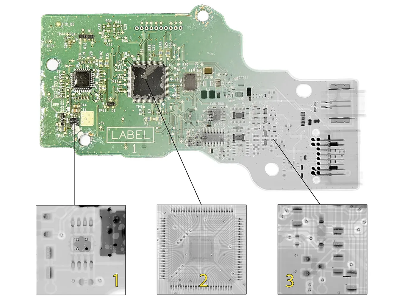
After reflow, inspect solder joints using X-ray imaging to detect voids or misalignment, especially for hidden connections like those in Ball Grid Arrays (BGAs). Automated Optical Inspection (AOI) can also catch surface-level defects like bridging or insufficient solder.
3. Control Environmental Factors
Moisture and contamination can ruin solder joints. Store PCBs and components in a controlled environment with low humidity (below 50% RH) and ensure cleanliness during assembly to prevent oxidation or flux residue issues.
4. Test for Reliability
Conduct thermal cycling and mechanical stress tests on assembled boards to simulate real-world conditions. For HDI designs, aim for solder joints that can withstand temperature cycles from -40°C to 125°C without cracking or delaminating.
Advanced Techniques for Solder Joint Reliability
For cutting-edge applications, consider these advanced methods to enhance solder joint formation in high-density PCBs:
1. Vacuum Reflow Soldering
Vacuum reflow reduces the formation of solder voids by removing trapped air during the soldering process. This technique is particularly effective for BGAs and other high-density components where voids can significantly impact performance.
2. Solder Preforms
In cases where precise solder volume is critical, solder preforms can be used alongside paste. These pre-shaped solder pieces ensure consistent joint thickness and are ideal for HDI designs with tight tolerances.
3. Selective Soldering for Mixed Assemblies
In high-density boards with mixed SMT and through-hole components, selective soldering targets specific areas without affecting nearby fine-pitch parts. This method offers precision and minimizes thermal stress.
Conclusion: Mastering Solder Joint Formation in High-Density PCBs
Achieving reliable solder joint formation in high-density PCB assembly is a complex but essential task. By understanding the challenges—such as working with fine-pitch components and managing thermal stress—you can take proactive steps to improve outcomes. Focus on critical factors like solder paste selection for HDI, tailored reflow profiling for high-density interconnect, and best practices like stencil optimization and advanced inspection.
With the insights and tips provided in this guide, you're well-equipped to tackle solder joint formation challenges head-on. Whether you're designing for consumer electronics, automotive systems, or industrial applications, prioritizing solder joint quality will ensure your high-density PCBs perform reliably under any condition. Keep refining your process, stay updated on new techniques, and watch your assemblies reach new levels of precision and durability.


