 ALLPCB


CEM-1 printed circuit boards use a cellulose-paper-reinforced epoxy laminate that offers a cost-effective option for many single-sided and simple double-sided designs. Electrical engineers often select this material when thermal demands remain moderate and budget constraints apply. Effective thermal management ensures components stay within safe operating ranges, preserving performance and extending product life. Poor heat dissipation in any PCB can lead to elevated junction temperatures, accelerated aging, and eventual failure. In CEM-1 boards the lower thermal conductivity of the base material compared with higher-performance laminates requires deliberate design attention from the earliest layout stages.
What Is CEM-1 PCB Thermal Management and Why It Matters
CEM-1 PCB thermal design encompasses the strategies and layout decisions that control heat flow from active components to the surrounding environment. The material's glass-transition temperature and thermal conductivity limit its ability to spread heat as efficiently as some alternatives, making targeted cooling techniques essential. Engineers must account for power dissipation, ambient conditions, and enclosure airflow when specifying board construction. Without proper temperature control, localized hot spots can exceed component ratings even when average board temperatures appear acceptable. Industry standards such as IPC-6012E guide qualification testing that includes thermal stress evaluations to verify board integrity under expected operating conditions.
Technical Principles of Heat Transfer in CEM-1 Boards
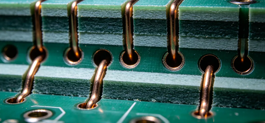
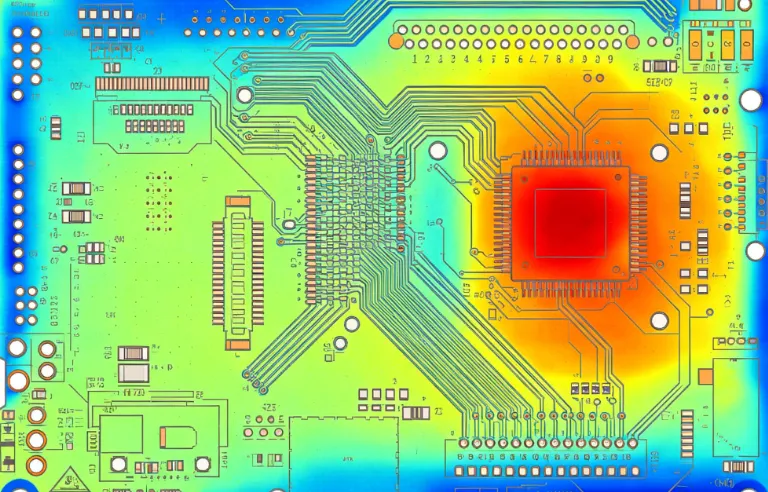
Heat generated by semiconductors and passive components travels through conduction within copper traces and planes, then moves to the board surface or attached hardware for convection and radiation. CEM-1's epoxy-paper core conducts heat less readily than glass-reinforced materials, so copper features must carry a larger share of the thermal load. Thermal resistance calculations consider trace thickness, via placement, and the contact area between components and the board. Elevated temperatures also influence material expansion, which can create mechanical stress at solder joints if coefficients of thermal expansion are not balanced during design. Engineers apply Fourier's law of conduction and basic convection correlations to predict temperature rises before prototyping. These calculations help identify whether additional measures such as thermal vias or external heat sinks will be required.
Practical Solutions and Best Practices for CEM-1 PCB Cooling Techniques
Layout practices that improve heat spreading include widening power and ground traces, adding solid copper pours beneath heat-generating devices, and positioning high-dissipation parts near board edges where airflow is stronger. Thermal vias placed in arrays under components provide low-resistance paths for heat to reach the opposite side of the board or an attached heat sink. Increasing copper weight on inner or outer layers further reduces thermal resistance without changing the base laminate. When component power exceeds what the board alone can handle, mechanical attachment of aluminum or copper heat sinks using thermally conductive adhesives or hardware becomes necessary. Airflow management through enclosure vents and fan placement complements these board-level measures. During assembly, solder mask openings around thermal pads ensure maximum contact area for heat transfer.
Designers verify these choices through thermal modeling and prototype testing that follows established qualification procedures. Standards such as JEDEC J-STD-020E address moisture sensitivity and reflow conditions that interact with thermal performance during manufacturing and operation. Regular review of component datasheets for maximum junction temperatures guides the selection of cooling methods appropriate to each device.
Troubleshooting Common Thermal Issues in CEM-1 Designs
Engineers frequently encounter excessive temperature rise when copper features are undersized or when components cluster without adequate spacing. Warpage can appear after repeated thermal cycling if the board's construction does not accommodate differential expansion. Measuring surface temperatures with thermocouples or infrared imaging during powered testing reveals hot spots that simulation may have missed. Adjusting via density, adding copper planes, or relocating parts often resolves these problems without changing the laminate choice. In cases where CEM-1 proves marginal, designers may evaluate alternative materials for future revisions while retaining the same thermal management principles.
Conclusion
CEM-1 PCB thermal design succeeds when engineers combine material-aware layout, strategic use of thermal vias and copper features, and appropriate external cooling hardware. Attention to heat flow paths from the schematic stage through final assembly maintains component reliability and prevents premature failures. Consistent application of these principles supports predictable performance across production volumes.
FAQs
Q1: How does CEM-1 PCB thermal design differ from FR-4 approaches?
A1: CEM-1 offers lower thermal conductivity, so designers rely more heavily on copper features and external cooling to achieve comparable temperature control. Thermal vias and enlarged copper areas become especially important to compensate for the base material properties while maintaining cost advantages.
Q2: What role do PCB thermal vias play in CEM-1 temperature control?
A2: Thermal vias create vertical heat paths through the board, allowing heat to reach additional copper layers or attached hardware. Arrays of vias under power components significantly lower thermal resistance and help keep junction temperatures within specification.
Q3: When should PCB heat sinks be added to CEM-1 boards?
A3: Heat sinks become necessary when component power dissipation exceeds the board's ability to dissipate heat through conduction and natural convection alone. Proper interface materials and secure mechanical attachment ensure effective heat transfer from the component package to the sink.
Q4: Which PCB cooling techniques work best for CEM-1 in enclosed systems?
A4: Forced airflow, strategic component placement near vents, and optimized copper pours provide the most reliable cooling in confined environments. Combining these board-level techniques with careful enclosure design maintains safe operating temperatures without requiring higher-grade laminates.
References
IPC-6012E — Qualification and Performance Specification for Rigid Printed Boards. IPC, 2017
JEDEC J-STD-020E — Moisture/Reflow Sensitivity Classification. JEDEC, 2014
IPC-TM-650 — Test Methods Manual. IPC (selected thermal test methods)


