ALLPCB


Overview
This article provides an introduction to capacitive touchscreen technology, covering electronic design and mechanical/structural design. The electronic design section includes principles and circuit design. The structural design section covers exterior structure, materials, and supplier processes.
Terminology
- V.A area: Visible area after assembly; no opaque traces or noticeable color differences are allowed.
- A.A area: Active area for operation; must meet mechanical and electrical performance requirements.
- ITO: Indium Tin Oxide, a conductive coating applied to film or glass.
- ITO film: Transparent PET film with conductive ITO layer.
- ITO glass: Conductive glass with ITO coating.
- OCA: Optically clear adhesive.
- FPC: Flexible printed circuit.
- Cover glass (lens): Decorative top cover glass.
- Sensor: The touch-sensing element located beneath the cover glass (film sensor or glass sensor).
Electronic Design
1. Introduction to Capacitive Touch Panels
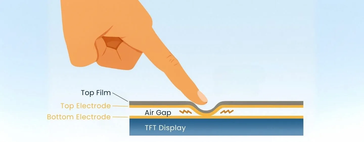
A capacitive touch panel (CTP) detects touch by using patterned ITO layers that form an X-Y capacitive matrix. When a finger touches the screen, scanning on the X and Y axes detects local capacitance changes and computes the touch coordinates.
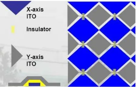
Figure 1 Capacitive distribution matrix
Capacitance Change Detection
Key definitions:
- ε0: Vacuum permittivity.
- ε1, ε2: Relative permittivity of different media.
- S1, d1, S2, d2: Areas and distances that form the capacitances.
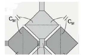
Figure 2 Schematic of capacitance distribution with and without touch
Without touch: C = Cm1 = ε1·ε0·S1/d1
With touch: C = Cm1*Cmg/(Cm1+Cmg), where Cm1 = ε1·ε0·S1/d1 and Cmg = ε2·ε0·S2/d2
The touch controller IC compares baseline (no-touch) capacitance to the measured capacitance to detect touch and determine position.
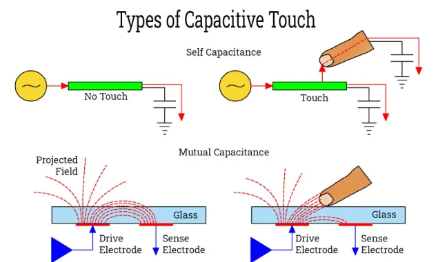
2. Self-Capacitance vs Mutual-Capacitance
Self-capacitance CTP measures the capacitance of individual electrodes relative to ground. Coordinates are obtained by scanning the horizontal and vertical electrode arrays separately and combining the changes. With a single touch point the coordinates are unique, but with two simultaneous touches self-capacitance can produce ambiguous "ghost" points, so true multi-touch is not supported.
Mutual-capacitance CTP measures capacitance between intersecting electrode pairs, with one axis transmitting excitation and the other axis sampling. This provides capacitance values for every intersection, enabling accurate detection of multiple simultaneous touch points. Therefore mutual-capacitance supports true multi-touch.
Self-capacitance advantages: simple, low computational load. Disadvantages: single-point only, slower response. Mutual-capacitance advantages: true multi-touch, faster. Disadvantages: more complex, higher power consumption, higher cost.
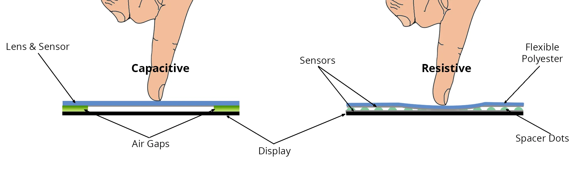
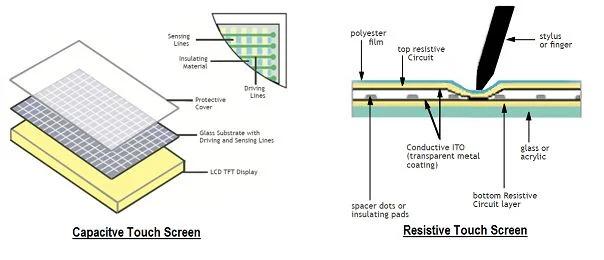
3. Structure and Materials
See the structural design section for detailed material choices and stack-ups.
Touch Controller IC
The touch controller IC handles touch data acquisition and processing. It samples the capacitance signals and uses an internal MCU to analyze and report touch information to the host.
IC pins and signals commonly include:
- Driver (TX): capacitive drive output lines.
- Sensor (RX): capacitive sense input lines.
- Power supplies: analog and digital rails. Typical analog voltage 2.6 V to 3.6 V (common values 2.8 V or 3.3 V). Digital I/O levels typically 1.8 V to 3.3 V, determined by the host. Designs may use single- or dual-supply configurations; single-supply is common to reduce pin count.
- GND: analog and digital ground; usually tied together but can be separated to reduce crosstalk.
- I2C interface: I2C_SCL (clock), I2C_SDA (data).
- SPI interface: SPI_SSEL (chip select, active low), SPI_SCK (clock), SPI_SDI (data input), SPI_SDO (data output).
- RESET: active-low reset.
- WACK: wake signal.
- TEXT_EN: test mode enable.
- GPIO0..N: general-purpose I/O.
- VREF: reference voltage.
- VDD5: internally generated 5 V supply.
Some ICs include additional special-purpose pins such as LED control, Sensor_ID, Key_Sensor. Refer to the specific IC datasheet for exact pin functions.
ITO Pattern Design
ITO can be etched into various patterns. There is no universally optimal pattern, because touch performance depends on interaction between the sensor design and the controller electronics.
The iPhone pattern is a simple design with horizontal electrodes on one side and vertical electrodes on the other, which requires precise manufacturing to form accurate interaction points.
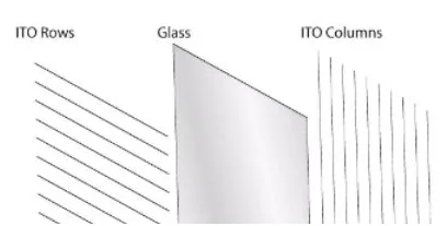
Figure 3 iPhone-style pattern
The common diamond-shaped closed-loop pattern uses 45-degree axes forming diamond blocks connected by small bridges. One glass carries row diamonds and the other carries column diamonds. Diamond size typically ranges from 4 mm to 8 mm and is compatible with most CTP controllers.
More complex patterns may require specialized controllers or licensing. Some IC vendors design proprietary patterns and may patent them to protect IP.
Common base ITO patterns include Diamond, Rectangle, Diamond & Rectangle, and Hexagon.
Layout Design Requirements
Driver IC placement methods include COF and COB.
COF (Chip on FPC): The IC is mounted on the FPC, allowing touchscreen modules to be changed without modifying the main board. This offers flexibility and compatibility with different controller ICs. Drawbacks include greater debugging work and longer procurement lead times.
COB (Chip on Board): The IC is mounted directly on the main board. Once the board and controller are fixed, changes are difficult because most controller ICs are not pin-to-pin compatible. COB offers lower cost, shorter lead time, and simpler supply chain, with less debugging workload.
Regardless of COF or COB, follow IC vendor recommendations and supplier best practices. Key layout considerations are summarized below.
1. Critical Component Placement
Place decoupling capacitors for each power rail close to the IC pins and keep traces short. The diagram below shows recommended component placement around the IC.
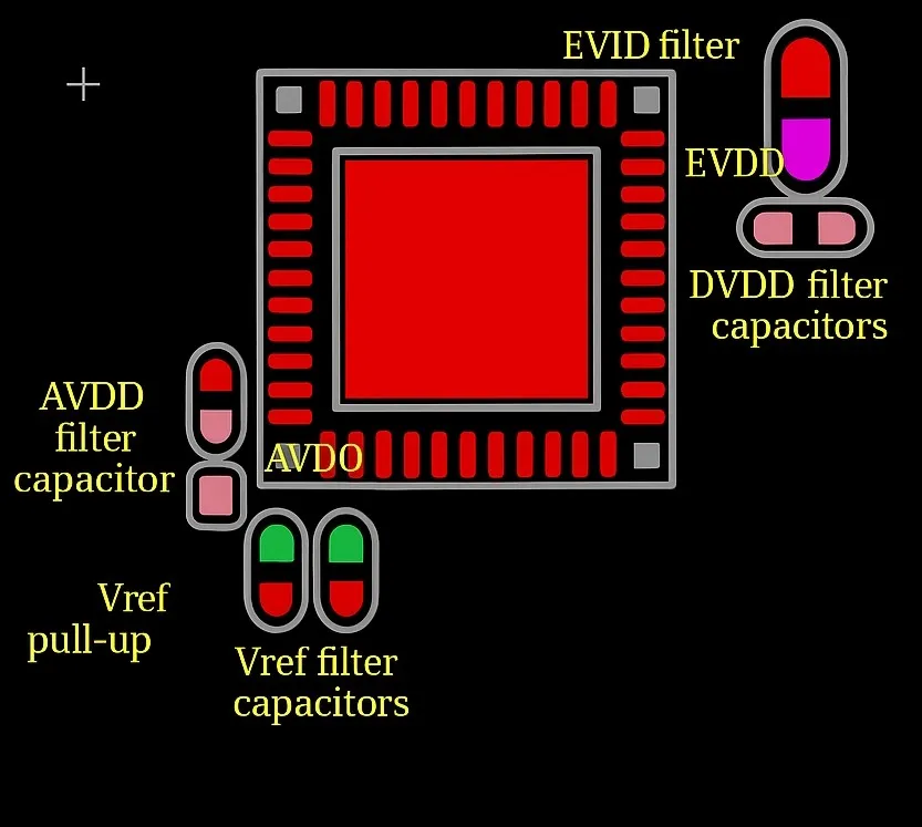
Figure 5 Example component placement
Avoid routing high-speed signals near the connector area between the touch panel and the main board.
For COB designs, locate the touch IC close to the host IC. Keep touch IC and FPC traces away from antennas such as FM, ADV, DTV, GSM, GPS, and BT. Place touch-related components inside a shield, preferably in their own shield can. If switching power supplies, RF circuits, or other logic are near the touch IC, use ground isolation to protect the touch IC, its power, and signal lines.
RF is the largest interference source in mobile devices. Maintain spacing between the touch IC and RF antennas: at least 20 mm at the top, and at least 10 mm at the bottom. These distances apply to both COF and COB layouts.
2. Routing
1) Power traces should be as short and wide as possible. Minimum width 0.2 mm, recommended ≥ 0.3 mm. Driver and sensor traces should be kept short to minimize loop area.
Unused driver or sensor channels on the controller should be left floating, not tied to ground or supply.
For COB designs, keep main-board traces short and as close as possible to the touchscreen connector. Provide test pads around the IC for driver and sensor signals to facilitate mass production testing, at least two pads per signal. Provide test pads for interfaces such as I2C, SPI, INT, and RESET for debugging.
2) Use ground traces to shield driver channels and prevent interference with sensitive signals such as Vref.
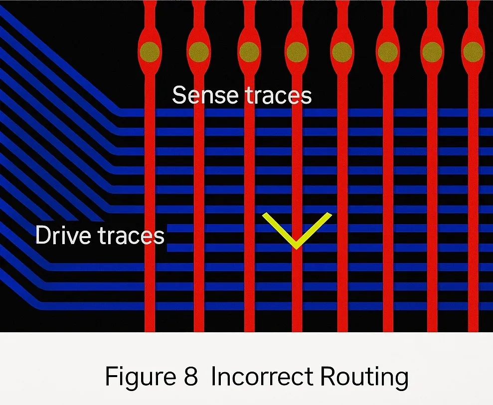
3) Route driver and sensor signal traces in parallel where possible and avoid crossing.
When traces are routed on different layers, avoid directly overlapping parallel traces on opposing layers, which can create unintended capacitance. Separate adjacent driver and sensor traces with a ground trace at least 0.2 mm wide.
If crossing of driver and sensor traces is unavoidable due to mechanical constraints, minimize the crossed area to reduce junction capacitance. Prefer perpendicular crossings and avoid multiple crossings. Use minimum trace widths for driver and sensor traces (0.07 mm to 0.08 mm).
For multi-layer COB designs, consider separating driver and sensor traces on different layers with ground shielding between them.
4) Avoid placing driver and sensor traces adjacent to communication traces such as I2C or SPI in parallel or crossing configurations to prevent pulse noise from corrupting measurement data. If communication traces must be nearby, shield them with ground traces.
3. Grounding and Shielding
The IC substrate must be grounded and include reliable ground vias; 4 to 8 vias are recommended. Place ground pads on both sides of driver and sensor compress points. Where space allows, place ground traces on both sides of driver and sensor routing, with recommended ground trace width ≥ 0.2 mm.
Unrouted areas of the FPC should be copper filled. Large-area copper helps reduce GND trace resistance and shields external interference. Use a grid-style copper pour to shield without significantly increasing capacitance between drive/sense traces and ground. Recommended grid: grid spacing 0.3 mm, track 0.1 mm. For FPCs that connect the sensor to the controller IC, copper fill on the back of signal traces and an additional grounded shielding film are recommended.
Provide at least two ground traces ≥ 0.2 mm between the FPC and the main control board to ensure reliable electrical grounding. If structure allows, reinforce with a steel plate; a reliably grounded steel plate improves shielding.
4. Design References
Key FPC dimensions should be considered during FPC design as shown below.
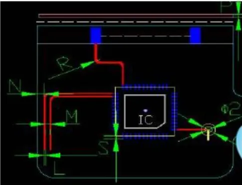
Key FPC dimension schematic
FPC routing should avoid right angles and sharp bends; use rounded arcs at bends. Reinforce component placement areas to facilitate SMD placement and soldering. Place vias primarily in reinforced areas; avoid vias in bend regions and adjacent areas. Mark reinforcement areas and total FPC thickness on drawings. Bending regions should not have reinforcement. Use a transition radius of R=1.0 mm between bend and component zones, and add copper traces at corners to improve strength and reduce tear risk.
Consider component area spacing during mechanical review to ensure sufficient structural space for components.
ESD Protection
ESD performance is a fundamental electrical requirement that affects product reliability and lifetime. For CTP designs, consider the following ESD protection recommendations:
- Maintain at least 3 mm clearance between FPC edges and any chassis openings or seams to avoid direct ESD discharge to the FPC.
- When possible, use grounded metal housings or ensure plastic housings have grounded conductive parts to improve ESD robustness.
- Some ICs or vendor solutions include TVS diodes or built-in ESD protection; select parts with appropriate ESD ratings where necessary.
- Use grid GND shielding on the FPC and, if necessary, a grounded shielding film to protect I2C and other signals from ESD coupling into the main board.
- Reduce the distance between VDD and GND to improve resistance to radiated ESD interference.
- Provide ground isolation around the ITO sensor area to prevent direct ESD interference with the sensor.
- Separate protection grounds: isolate IC supply ground and FPC protective ground, ensuring thorough connections around the IC to prevent ESD from directly impacting the IC.
Technical Outlook
As capacitive touch panels become more widely used, standardization and interoperability are important industry directions.
Technical development trends include:
- Controller integration: combining LCM and CTP driving functions into unified solutions.
- Thinner glass panels: integrating CTP sensors on the LCD surface or embedding sensors in-cell to achieve thinner, lighter displays.
Structural Design
1. Stackups and Materials
Common stack structures include:
G+F (Cover Glass + Film Sensor)
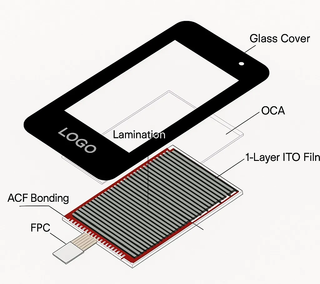
Structure: cover glass + film sensor.
Characteristics: single-layer film sensor with triangular ITO pattern, primarily single-touch with virtual two-finger gestures possible.
Advantages: low tooling cost, high cost-effectiveness, lowest unit cost among capacitive TP structures, thin overall thickness, good transmittance, short lead time, interchangeable cover shape.
Drawbacks: mainly single-point, poor handwriting performance, virtual two-finger gestures have limited accuracy.
G+F+F (Cover Glass + Film Sensor + Film Sensor)
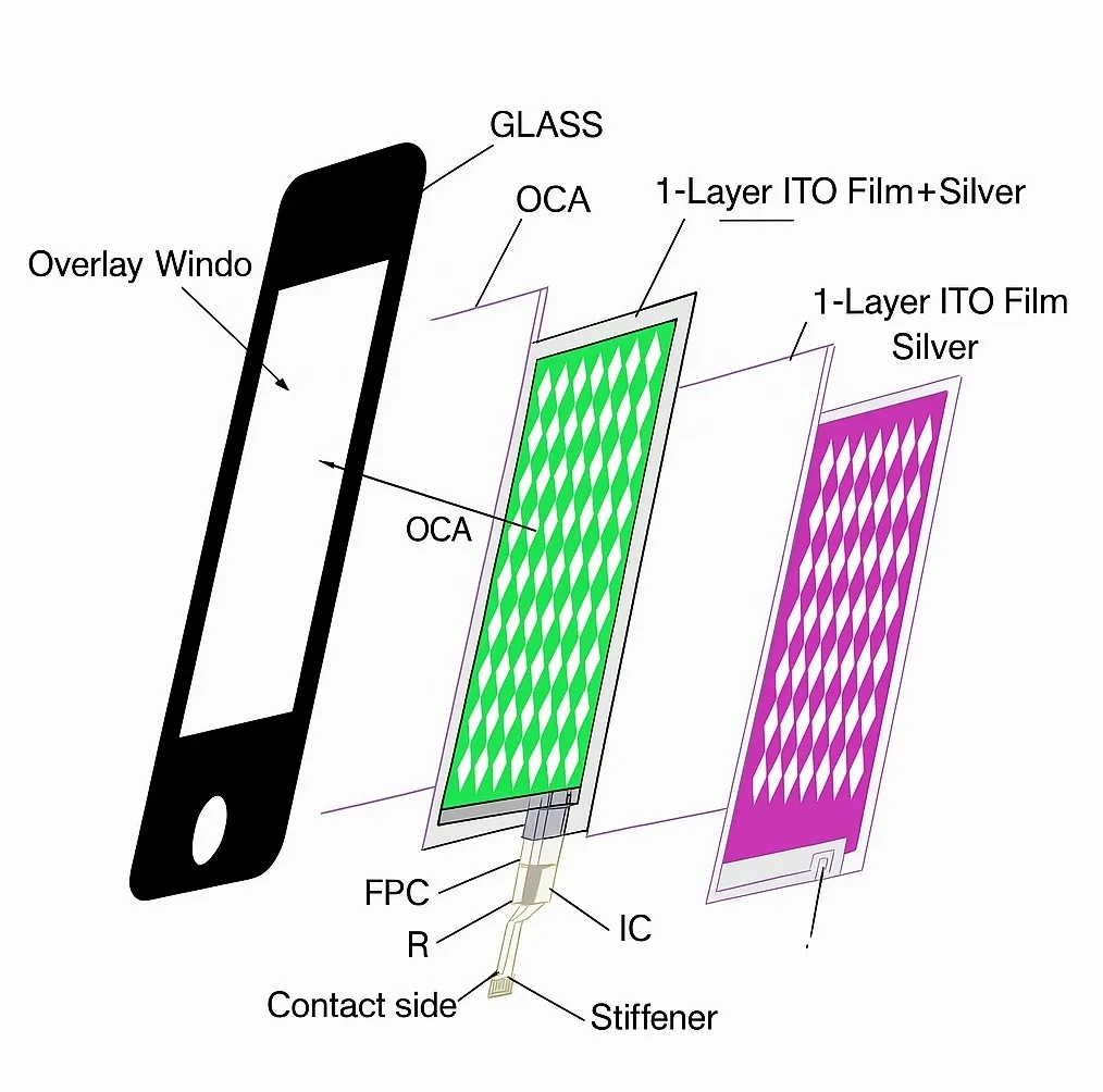
Structure: cover glass + two film sensors.
Characteristics: two-layer film sensors with diamond ITO pattern supporting true multi-touch.
Advantages: high accuracy, good handwriting performance, supports true two-finger gestures, interchangeable cover shape.
Drawbacks: slightly lower transmittance (about 5% less than G/G), higher cost than G/F but lower than G/G.
G+G (Cover Glass + Glass Sensor)
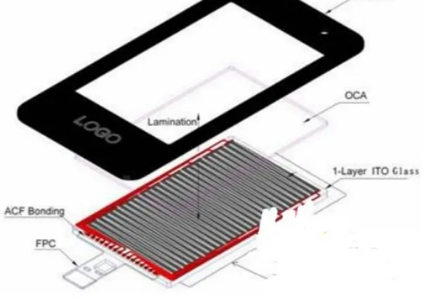
Structure: cover glass + glass sensor.
Characteristics: single-layer glass sensor with diamond ITO pattern, supporting true multi-touch.
Advantages: high accuracy, good transmittance, good handwriting performance, reliable and long service life, interchangeable cover shape.
Drawbacks: rear glass sensor is vulnerable to impact, higher development cost and longer cycles, limited replaceability.
2. Materials
- ITO glass: Indium Tin Oxide coated glass produced via vacuum deposition, typically with a SiO2 base layer and an ITO conductive layer; offers high visible light transmittance and conductivity.
- Glass sensor thickness options: 0.33 mm, 0.4 mm, 0.55 mm.
- ITO film: commonly 0.125 mm thick.
- OCA: available in thicknesses such as 50 μm, 100 μm, 150 μm, 200 μm, 250 μm, 300 μm; common suppliers include 3M, Hitachi Chemical, and Mitsubishi Resin.
- Cover glass: chemically or thermally strengthened glass with thicknesses such as 0.55 mm, 0.7 mm, 0.8 mm, 0.95 mm, 1.0 mm, 1.1 mm; surface hardness typically around 7H.
- PMMA: recommended thickness at or above 1.0 mm; maintain at least 0.5 mm gap between LCM and CTP.