If you're looking to master copper pour design rules for your PCB layout, you're in the right place. Copper pours are essential for enhancing electrical performance, managing heat, and reducing noise in printed circuit boards (PCBs). In this guide, we'll cover the critical rules and best practices for copper pour design, focusing on clearances, spacing, and maintaining signal integrity. Whether you're a beginner or a seasoned engineer, this comprehensive resource will help you create reliable and efficient PCB designs.
Let's dive into the details of copper pour design, exploring how to apply these rules effectively to optimize your PCB layouts for performance and manufacturability.
What Is a Copper Pour in PCB Design?
A copper pour, often called a copper fill or copper flooding, is a large area of copper that covers unused spaces on a PCB. It acts as a ground plane, power plane, or heat sink, depending on its purpose. By filling empty areas with copper, you can improve electrical conductivity, reduce electromagnetic interference (EMI), and balance copper distribution for manufacturing.
Copper pours are vital for maintaining signal integrity in high-speed designs and ensuring proper grounding. However, without following proper copper pour design rules, you risk issues like short circuits, excessive noise, or uneven heat distribution. Let's explore the fundamental guidelines to get it right.
Why Are Copper Pour Design Rules Important?
In PCB layout, copper pours serve multiple purposes, but they must be implemented correctly to avoid problems. Poorly designed copper pours can lead to signal crosstalk, unintended shorts, or manufacturing defects. Following strict copper pour design rules ensures:
- Signal Integrity: A well-designed copper pour reduces noise and maintains consistent impedance for high-speed signals, often targeting values like 50 ohms for controlled impedance traces.
- Thermal Management: Copper pours dissipate heat from components, preventing hotspots that could damage the board.
- Manufacturability: Balanced copper distribution prevents warping during fabrication and improves etching accuracy.
- EMI Reduction: Ground planes created by copper pours shield sensitive traces from interference.
By adhering to rules for clearances and spacing, you can avoid common pitfalls and ensure your design performs as intended.
Key Copper Pour Design Rules for PCB Layout
Designing copper pours requires attention to detail. Below, we break down the essential rules to follow for a successful PCB layout.
1. Maintain Proper Clearances
Clearances refer to the minimum distance between a copper pour and other elements like traces, pads, or vias. Inadequate clearance can cause short circuits or electrical interference. Here are some guidelines:
- Set a minimum clearance of at least 0.2 mm (8 mils) between copper pours and unrelated traces or components for low-voltage designs. For high-voltage applications, increase this to 0.5 mm (20 mils) or more, depending on the voltage rating.
- Ensure clearances comply with your design's voltage and safety standards, such as IPC-2221, which provides spacing guidelines based on voltage levels (e.g., 0.6 mm for 50V).
- Use design rule checks (DRC) in your PCB software to automatically flag clearance violations.
Proper clearance prevents accidental connections and maintains electrical isolation, especially in dense layouts.
2. Define Appropriate Spacing for Signal Integrity
Spacing is critical for maintaining signal integrity, especially in high-speed designs where signals can reach speeds of 1 GHz or higher. Copper pours often act as reference planes for signals, so their placement affects impedance and noise levels.
- Keep high-speed traces close to a continuous copper pour (ground or power plane) to maintain a consistent return path. A typical spacing between a trace and its reference plane might be 0.1 mm (4 mils) in a multilayer board to achieve 50-ohm impedance.
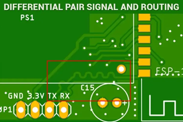
- Avoid splitting copper pours under high-speed differential pairs, as this can disrupt the return path and introduce noise.
- For multilayer PCBs, ensure spacing between layers with copper pours is uniform to prevent impedance mismatches.
By controlling spacing, you can minimize crosstalk and ensure clean signal transmission across your board.
3. Connect Copper Pours to the Correct Net
Always connect copper pours to the appropriate net, such as ground (GND) or a specific power rail (e.g., 3.3V). Unconnected or "floating" copper areas can act as antennas, picking up noise and degrading signal integrity.
- Use vias or thermal reliefs to connect copper pours to the desired net. For ground planes, place multiple vias (e.g., spaced every 10 mm) to ensure low-impedance connections.
- Avoid connecting a copper pour to multiple nets, as this can create unintended shorts or noise loops.
- Label the pour clearly in your design software to avoid confusion during layout or manufacturing.
Proper net connections are a cornerstone of effective copper pour design, ensuring functionality and reducing EMI.
4. Use Thermal Reliefs for Pads and Vias
When a copper pour connects to component pads or vias, use thermal reliefs to prevent soldering issues. Thermal reliefs are small copper spokes that connect the pad to the pour, reducing heat dissipation during soldering.
- Set thermal relief width to about 0.25 mm (10 mils) and use 4 spokes per pad for balanced heat distribution.
- For high-current applications, consider increasing spoke width to 0.5 mm (20 mils) to handle more current without overheating.
- Ensure thermal reliefs don't compromise the connection to the pour, especially for ground planes critical to signal integrity.
Thermal reliefs make assembly easier and prevent cold solder joints, especially on large copper areas.
5. Balance Copper Distribution for Manufacturing
Uneven copper distribution can cause PCB warping or etching inconsistencies during manufacturing. Copper pours help balance the copper density across the board, but they must be applied thoughtfully.
- Aim for a copper density of 50-70% on each layer to avoid manufacturing issues. If one area has dense traces, use a copper pour in empty spaces to balance it out.
- For outer layers, consider adding "copper thieving"—small, unconnected copper shapes in empty areas—to even out density without affecting the circuit.
- Coordinate with your fabrication house to understand their specific copper balance requirements.
Balanced copper distribution ensures your PCB remains flat and meets manufacturing tolerances.
Advanced Tips for Copper Pour Design and Signal Integrity
Beyond the basics, there are advanced strategies to optimize copper pours for high-performance designs. These tips focus on enhancing signal integrity and addressing complex PCB layout challenges.
6. Use Via Stitching for Ground Planes
In multilayer PCBs, via stitching connects copper pours across layers, creating a low-impedance path for ground or power. This technique is especially useful for maintaining signal integrity in high-speed designs.
- Place stitching vias at regular intervals, such as every 5-10 mm, around the board's perimeter or near high-speed signals.
- Ensure via size matches current requirements—use 0.3 mm (12 mils) diameter vias for standard applications or larger for high-current designs.
- Avoid placing stitching vias too close to signal traces to prevent unintended coupling.
Via stitching reduces ground bounce and ensures a solid reference plane for signals.
7. Avoid Copper Pours Near Sensitive Analog Circuits
While copper pours are great for digital circuits, they can introduce noise in sensitive analog areas. For mixed-signal designs, keep copper pours away from analog components or use separate ground planes.
- Maintain a clearance of at least 1 mm (40 mils) between analog traces and digital ground pours to minimize interference.
- Use split planes to isolate analog and digital grounds, connecting them at a single point to avoid ground loops.
- Route sensitive analog signals over their own dedicated reference plane for optimal performance.
Thoughtful separation preserves the accuracy of analog signals in mixed-signal layouts.
8. Simulate and Test Your Design
Before finalizing your PCB layout, use simulation tools to analyze the impact of copper pours on signal integrity and EMI. Many design software packages offer built-in simulation features to predict performance.
- Check for impedance mismatches in high-speed traces, targeting values like 50 ohms for single-ended signals or 100 ohms for differential pairs.
- Simulate EMI to identify potential noise sources caused by copper pour placement.
- Perform a physical prototype test to validate simulation results, especially for critical designs.
Simulation and testing catch issues early, saving time and cost in the design process.
Common Mistakes to Avoid in Copper Pour Design
Even experienced designers can make errors when applying copper pours. Here are some common mistakes to watch out for:
- Floating Copper Pours: Unconnected pours act as noise antennas, degrading performance. Always tie pours to a net.
- Insufficient Clearance: Too little spacing between pours and traces can cause shorts or arcing, especially in high-voltage designs.
- Overusing Copper Pours: Flooding every empty space without purpose can increase parasitic capacitance and affect signal timing.
- Ignoring Thermal Reliefs: Skipping thermal reliefs on pads makes soldering difficult and risks poor connections.
By avoiding these pitfalls, you can ensure your copper pour design enhances rather than hinders your PCB's performance.
Conclusion: Mastering Copper Pour Design for PCB Success
Applying copper pour design rules is essential for creating reliable and high-performing PCB layouts. By focusing on clearances, spacing, and signal integrity, you can optimize your designs for electrical performance, thermal management, and manufacturability. From maintaining proper clearances of 0.2 mm or more to using via stitching for ground planes, every detail matters in achieving a robust design.
Whether you're working on a simple single-layer board or a complex multilayer design, these guidelines will help you navigate the challenges of copper pour implementation. Use simulation tools, follow industry standards, and balance copper distribution to ensure your PCB meets both functional and manufacturing requirements.
With these best practices in hand, you're well-equipped to tackle your next PCB layout project with confidence. Keep refining your skills, and your designs will stand out for their quality and reliability.
 ALLPCB


