 ALLPCB


Introduction
Laser drilling techniques have transformed PCB fabrication by enabling the creation of microvias essential for high-density interconnect (HDI) boards. These methods use focused laser beams to ablate precise holes in dielectric materials and copper layers, supporting finer pitches and denser routing in modern electronics. As electric engineers demand higher performance from compact designs, understanding advanced laser drilling becomes critical for reliable PCB manufacturing. This article explores the principles, techniques, challenges, and best practices aligned with factory processes. Factory-driven insights reveal how these techniques address the limitations of mechanical drilling, particularly for vias under 150 microns. By optimizing laser parameters, manufacturers achieve superior hole quality and plating reliability in production environments.
What Are Laser Drilling Techniques and Why They Matter in PCB Fabrication
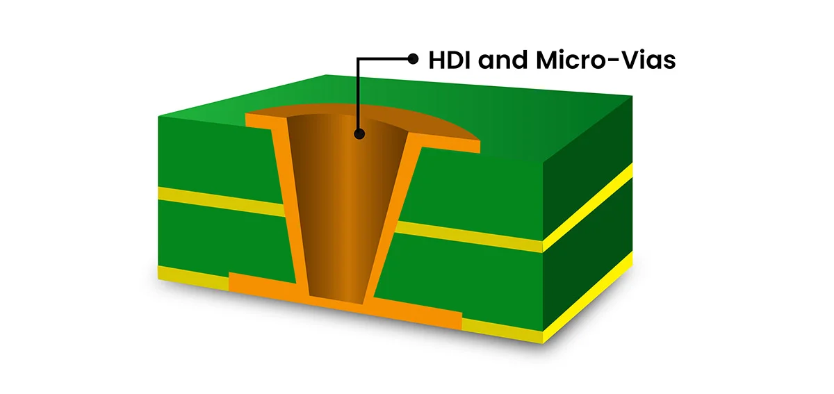
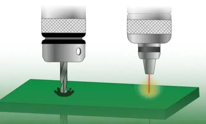
Laser drilling techniques involve directing a high-energy laser beam to vaporize targeted materials, forming blind, buried, or stacked microvias without physical contact. Unlike mechanical drilling, which struggles with holes below 150 microns due to bit wear and vibration, laser methods excel in precision and speed for HDI applications. Microvias, defined as holes 150 microns or smaller with an aspect ratio of 1:1 or less, connect adjacent layers efficiently, enabling board sizes to shrink while increasing layer count. In PCB fabrication, these techniques support via-in-pad designs for fine-pitch BGAs, where traditional vias cannot fit under components. Factory experience shows laser drilling processes thousands of vias per minute, reducing cycle times compared to mechanical alternatives. This relevance grows with demands for 0.5 mm pitch packages and beyond, where microvia reliability directly impacts signal integrity and thermal management.
The shift to laser drilling stems from its ability to handle diverse materials like FR-4, polyimide, and buildup films such as ABF or RCC, which are optimized for ablation. CO2 lasers dominate for dielectric removal, while UV lasers tackle copper and finer features. These techniques align with IPC-2226 guidelines for HDI designs, specifying microvia diameters of 75-150 microns and capture pads 200-350 microns. Engineers benefit from non-contact processing that minimizes delamination risks during sequential lamination cycles. Ultimately, mastering laser drilling techniques ensures manufacturability for advanced PCBs used in telecommunications, automotive, and computing sectors.
Technical Principles of Laser Drilling for Microvias
The core principle of laser drilling relies on thermal ablation, where photon energy breaks molecular bonds in the target material, vaporizing it into gas and ejecting residue via recoil pressure. CO2 lasers, operating at 10.6 micron infrared wavelength, absorb strongly in organic dielectrics like epoxy, creating clean holes 50-150 microns in diameter but reflecting off copper, necessitating prior etching or UV preprocessing. UV lasers, such as frequency-tripled Nd:YAG at 355 nm, penetrate both copper and dielectrics with minimal heat-affected zones (HAZ), focusing to 12-50 microns for sub-100 micron vias. Pulse characteristics—energy (5-20 W), duration (10-50 ns), and repetition (50-100 kHz)—control ablation depth and wall roughness, with shorter pulses reducing carbonization.
Drilling modes include percussion, where multiple stationary pulses deepen the hole; trepanning, circling the beam for larger diameters; and helical spiraling for uniform enlargement. In HDI fabrication, sequential lamination builds layers, drilling microvias layer-by-layer to maintain aspect ratios of 0.75:1 to 1:1, ensuring even plating. Material homogeneity is vital, as glass fibers in FR-4 can protrude, requiring desmear processes like plasma cleaning. Target copper thickness should exceed top copper by at least double to act as a natural stop layer, preventing over-drilling. Factory alignment systems use fiducials for ±10 micron accuracy, critical for stacked configurations per IPC-2226 microvia rules.[[2]](https://pcbsync.com/ipc-2226)
Advanced Laser Drilling Techniques
Advanced techniques combine laser types for hybrid processing: UV lasers first clear entry copper, CO2 ablates dielectric to the landing pad, and a final UV pass removes residue, yielding smooth tapered walls ideal for plating. Ultrashort pulse lasers (picosecond or femtosecond) further minimize HAZ by confining energy to the focal point, enabling vias as small as 50 microns in high-Tg laminates. Stacked microvias, limited to 2-3 per IPC-2226 for reliability, use copper-filled and planarized structures, with voids under 25% to avoid electromigration failures. Staggered vias offset alignments reduce stress, while via-in-pad eliminates fanouts for 0.4-0.5 mm BGA pitches.
Helical and burst-mode drilling enhance throughput, projecting shaped beams for faster field processing in production panels. For coreless HDI (Type V), full buildup relies on precise depth control without cores. Factory optimization tailors parameters per material: higher power for polyimide, lower repetition for ABF to prevent fiber pullout. These advanced techniques support 20+ layer HDI with microvia-to-microvia spacing of 50-100 microns, clearances to traces at 25 microns minimum. Integration with direct imaging ensures fiducial-based registration across cycles.
Laser Drilling Challenges and Mitigation Strategies
Laser drilling challenges include thermal damage like charring or delamination from excessive HAZ, particularly with CO2 on thicker dielectrics. Tapering occurs due to beam divergence, widening holes bottom-up and risking plating voids at high aspect ratios over 1:1. Debris and carbon residue hinder adhesion, while misalignment from stack-up variations causes open circuits. Depth inconsistency arises in heterogeneous materials, where epoxy vaporizes faster than glass, leaving protrusions.
Mitigation starts with parameter tuning: short pulses and optimal focus for straight walls, plasma desmear for residue removal. Homogeneous dielectrics like RCC minimize absorption variances. Sequential drilling per layer controls depth, adhering to IPC-6012 qualification for via performance.[[1]](https://www.protoexpress.com/blog/how-does-laser-drilling-work-pcbs) Advanced imaging and calibration address alignment, while thin foils (≤18 μm copper) aid penetration. Factory plasma cleaning post-drill ensures IPC-A-600 acceptability criteria for wall roughness.
Best Practices for Laser Drilling in PCB Manufacturing
Implement design for manufacturability (DFM) by specifying laser-drillable materials and limiting stacks to 2-3 vias. Maintain dielectric thickness 50-100 microns for 0.75:1 aspect ratios, with capture pads 50-75 microns oversized. Calibrate equipment regularly on test coupons, verifying ±10 micron tolerances. Post-drill desmear and plating sequence ensures barrel integrity. Collaborate on stack-ups to match factory capabilities, avoiding glass-heavy cores.
Conclusion
Advanced laser drilling techniques enable precise microvia formation critical for HDI PCB fabrication, overcoming mechanical limits while addressing key challenges through optimized processes. Factory adherence to parameters and standards delivers reliable, high-yield production. Engineers leveraging these insights achieve denser, performant boards.
FAQs
Q1: What are the main laser drilling techniques for microvias in PCB fabrication?
A1: CO2 lasers ablate dielectrics for 100-150 micron holes, while UV lasers handle copper and smaller features under 100 microns. Percussion and helical modes control depth and shape, with hybrid sequences for clean walls. These techniques support HDI microvias per IPC-2226, ensuring plating quality in production.
Q2: How do laser drilling challenges impact PCB reliability?
A2: Challenges like HAZ, tapering, and residue can cause plating voids or opens, reducing reliability in stacked microvias. Mitigation via desmear and parameter optimization maintains aspect ratios under 1:1. Factory processes align with IPC-6012 for performance verification.
Q3: What aspect ratios are recommended for laser-drilled microvias?
A3: Preferred 0.75:1 to 1:1, with dielectric 50-100 microns matching hole diameters of 75-150 microns. Higher ratios risk incomplete plating; thin layers and sequential buildup ensure compliance in advanced techniques.
Q4: When should electric engineers choose laser over mechanical drilling?
A4: Opt for laser when vias under 150 microns, blind/buried needs, or HDI densities require precision without vibration damage. Mechanical suits larger through-holes; laser excels in microvia challenges for compact designs.
References
IPC-2226 — Sectional Design Standard for HDI Printed Boards. IPC.
IPC-6012E — Qualification and Performance Specification for Rigid Printed Boards. IPC, 2015.
IPC-A-600K — Acceptability of Printed Boards. IPC, 2020.


