ALLPCB


If you're looking to achieve optimal solder paste printing on OSP-finished PCBs, you're in the right place. OSP (Organic Solderability Preservative) is a popular surface finish for printed circuit boards due to its cost-effectiveness and eco-friendly nature. However, its unique properties require specific techniques for effective solder paste application. In this comprehensive guide, we'll walk you through the essentials of OSP solder paste printing, PCB stencil design, and best practices for SMT stencil application to ensure high-quality results in your surface mount technology (SMT) assembly process.
What is OSP Finish and Why Does It Matter for Solder Paste Printing?
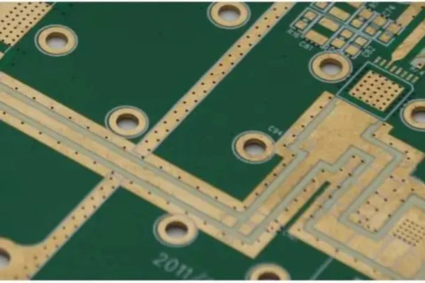
OSP is a thin organic coating applied to the copper pads of a PCB to protect them from oxidation before soldering. Unlike other finishes like HASL (Hot Air Solder Leveling) or ENIG (Electroless Nickel Immersion Gold), OSP is a non-metallic layer that gets removed during the soldering process to expose clean copper for bonding. This unique characteristic makes OSP ideal for fine-pitch components and high-density designs, but it also poses challenges for solder paste printing.
The organic layer of OSP can sometimes interfere with the adhesion and spread of solder paste if not handled properly. This is why understanding OSP solder paste printing techniques and optimizing PCB stencil design are critical for achieving consistent and reliable solder joints. Let's dive into the key factors that influence the process and how to address them for optimal outcomes.
Key Challenges in OSP Solder Paste Printing
Before we explore solutions, it's important to recognize the challenges associated with solder paste application on OSP-finished PCBs. Here are the primary hurdles:
- Surface Sensitivity: The organic layer on OSP-finished PCBs can degrade under high temperatures or prolonged exposure to air, affecting solder paste adhesion.
- Wettability Issues: OSP provides good wettability when fresh, but if the coating is compromised, it can lead to poor solder joint formation.
- Stencil Alignment: Misalignment during solder paste printing can result in uneven deposits, especially on fine-pitch components commonly used with OSP finishes.
- Paste Volume Control: Over- or under-application of solder paste can cause defects like bridging or insufficient solder, which are more pronounced on OSP due to its flat surface.
Addressing these challenges starts with a well-thought-out approach to PCB stencil design and solder paste application techniques tailored for OSP finishes.
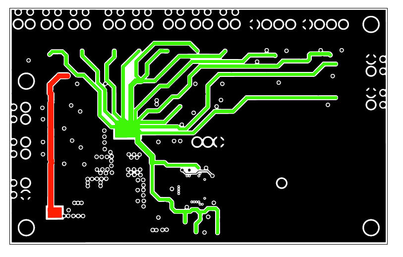
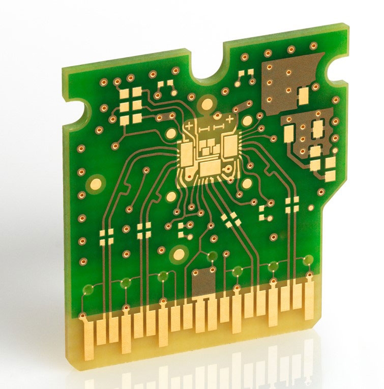
Optimizing PCB Stencil Design for OSP Solder Paste Printing
A well-designed stencil is the foundation of effective solder paste printing, especially for OSP-finished PCBs. The stencil controls the amount and placement of solder paste, directly impacting the quality of solder joints. Here are key considerations for OSP stencil design:
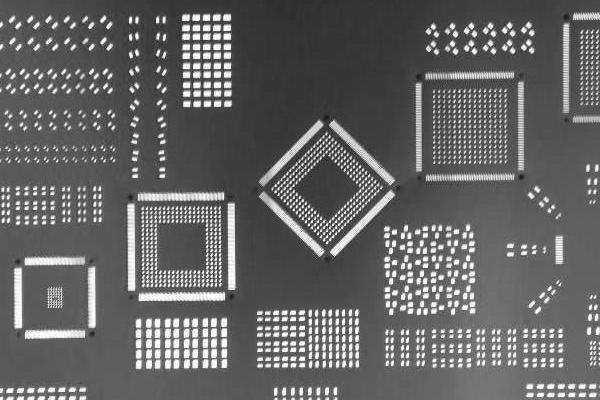
1. Aperture Size and Shape
The openings (apertures) in the stencil must match the pad sizes on the PCB. For OSP-finished boards, which often feature fine-pitch components, reducing aperture size by 10-20% compared to the pad size can help prevent excessive paste deposition and reduce the risk of bridging. For example, if a pad measures 0.5 mm x 0.5 mm, consider an aperture of 0.4 mm x 0.4 mm. Rounded corners on apertures also improve paste release, ensuring cleaner deposits.
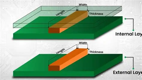
2. Stencil Thickness
Stencil thickness determines the volume of solder paste applied. For OSP PCBs with small components, a thinner stencil (typically 0.1 mm to 0.12 mm) is ideal for controlling paste volume. Thicker stencils (0.15 mm or more) may lead to excess paste, increasing the risk of defects like solder balls. Choose the thickness based on the smallest component on your board to maintain consistency across the design.
3. Material and Manufacturing Quality
Opt for stainless steel stencils with laser-cut apertures for precision, especially when working with OSP finishes. High-quality stencils ensure smooth edges on apertures, reducing the likelihood of paste sticking or uneven application. Electropolishing the stencil surface can further enhance paste release, which is critical for the flat, non-metallic surface of OSP.
Best Practices for Solder Paste Application on OSP-Finished PCBs
With a properly designed stencil in hand, the next step is mastering the solder paste application process. Here are actionable tips for achieving optimal results with OSP solder paste printing:
1. Control Environmental Conditions
OSP coatings are sensitive to humidity and temperature. Store OSP-finished PCBs in a controlled environment (ideally 20-25°C and 40-60% relative humidity) to prevent degradation of the organic layer. During printing, maintain similar conditions in the assembly area to ensure consistent paste behavior. High humidity can cause the paste to absorb moisture, leading to defects like voids in solder joints.
2. Use the Right Solder Paste
Choose a solder paste with a formulation suited for OSP finishes. Type 4 or Type 5 pastes, which have smaller particle sizes (20-38 microns for Type 4 and 15-25 microns for Type 5), are ideal for fine-pitch components often found on OSP boards. These pastes provide better print resolution and reduce the risk of clogging in small stencil apertures. Additionally, select a no-clean flux paste to minimize residue that could interact with the OSP layer.
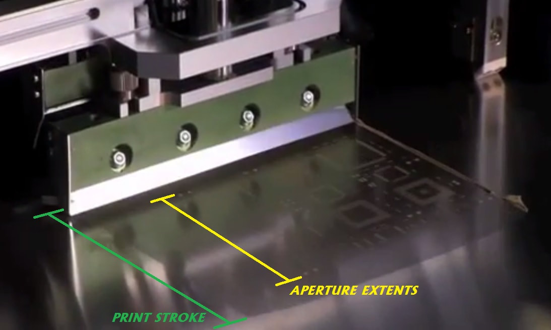
3. Optimize Printing Parameters
Adjust the settings on your solder paste printer for precision. Key parameters include:
- Squeegee Pressure: Use moderate pressure (around 8-12 kg for a 300 mm squeegee) to avoid damaging the OSP layer while ensuring full aperture fill.
- Print Speed: A slower speed (20-40 mm/s) allows for better paste transfer, especially for fine-pitch designs.
- Separation Speed: Set a slow separation speed (0.5-1.0 mm/s) between the stencil and PCB to prevent paste smearing or sticking.
4. Inspect and Clean Regularly
After each print cycle, inspect the stencil for paste buildup and clean it using an appropriate solvent or under-stencil wiping system. Residue on the stencil can lead to inconsistent deposits, which are more noticeable on OSP finishes due to their flat surface. Regular inspection of the PCB after printing using automated optical inspection (AOI) systems can also help catch defects early.
Advanced Tips for SMT Stencil Application with OSP
For engineers looking to take their OSP solder paste printing to the next level, consider these advanced strategies during SMT stencil application:
1. Implement Step Stencils for Mixed Components
If your OSP PCB features a mix of large and small components, a step stencil can be a game-changer. This type of stencil has varying thicknesses in different areas, allowing more paste for larger components (e.g., connectors) and less for fine-pitch ICs. For instance, a step stencil might have a 0.15 mm thick area for power components and a 0.1 mm thick area for QFN packages, ensuring optimal paste volume across the board.
2. Use 3D Solder Paste Inspection (SPI)
Investing in a 3D SPI system can significantly improve quality control. These systems measure the height, area, and volume of solder paste deposits after printing, ensuring they meet design specifications. For OSP-finished PCBs, where paste volume control is critical, 3D SPI can detect issues like insufficient paste (leading to weak joints) or excess paste (causing bridging) before reflow soldering. Typical targets for paste height are 80-120 microns for fine-pitch components.
3. Minimize Time Between Printing and Reflow
The OSP layer can degrade if exposed to air for too long after solder paste application. Aim to move the PCB to the reflow oven within 4-6 hours of printing. If delays are unavoidable, store the printed boards in a nitrogen-purged environment to slow oxidation and preserve the integrity of both the OSP coating and the solder paste.
Troubleshooting Common Issues in OSP Solder Paste Printing
Even with the best practices in place, issues can arise during solder paste printing on OSP-finished PCBs. Here are solutions to common problems:
- Uneven Paste Deposits: Check for stencil misalignment or inconsistent squeegee pressure. Ensure the printer is calibrated and the stencil is clean.
- Poor Wettability: If solder doesn't spread properly during reflow, the OSP layer may be degraded. Verify storage conditions and minimize exposure time before soldering.
- Solder Bridging: Reduce aperture size or stencil thickness to control paste volume. Adjust print speed and pressure for better control.
- Insufficient Solder: Increase stencil thickness slightly or check if the solder paste has the correct viscosity for your application.
Benefits of Mastering OSP Solder Paste Printing
Getting solder paste printing right on OSP-finished PCBs offers several advantages for your SMT assembly process:
- Improved Reliability: Precise paste application leads to consistent solder joints, reducing the risk of failures in the field.
- Cost Efficiency: OSP is a low-cost surface finish, and optimizing printing reduces material waste and rework expenses.
- Environmental Friendliness: OSP is lead-free and compliant with RoHS standards, making it a sustainable choice for modern electronics.
- Support for High-Density Designs: Fine-tuned stencil design and printing techniques enable the use of OSP in complex, high-density PCB layouts.
Conclusion: Elevate Your OSP Solder Paste Printing with Precision
Achieving optimal solder paste printing on OSP-finished PCBs requires a combination of thoughtful PCB stencil design, precise solder paste application, and strict control over environmental and process parameters. By focusing on aperture optimization, stencil quality, and advanced techniques like 3D SPI, you can overcome the unique challenges of OSP finishes and ensure high-quality solder joints for your SMT assemblies.
Whether you're working on fine-pitch components or mixed designs, the tips and strategies outlined in this guide will help you refine your process for consistent, reliable results. Start by evaluating your current stencil design and printing setup, and make incremental adjustments based on the recommendations provided. With the right approach, OSP solder paste printing can become a seamless and efficient part of your PCB manufacturing workflow.