My Message
 Suggestions


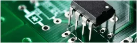
In the PCB design, wiring is an important step to complete the product design. It can be said that the previous preparation work is done for it. In the whole PCB, the wiring design process is the highest, the trick is the finest, and the workload is the largest.
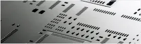
PCB wiring has single-sided wiring, double-sided wiring, and multilayer wiring. There are also two ways of wiring: automatic routing and interactive wiring. Before automatic routing, you can use interactive pre-wired lines that require more stringent requirements.
The edges of the input and output should avoid adjacent parallel to avoid reflection interference. If necessary, ground wire should be isolated. The wiring of two adjacent layers should be perpendicular to each other, and parasitic coupling is easy to occur in parallel.
The routing rate of automatic routing depends on a good layout, and the wiring rules can be preset, including the number of bending of the traces, the number of vias, and the number of steps.
Generally, the exploratory warp line is firstly connected, and the short lines are quickly connected, and then the labyrinth wiring is performed. First, the wiring to be cloth is optimized for the global routing path, and the laid line can be disconnected as needed. And try to re-route to improve the overall effect.
For the current high-density PCB design, it has been felt that the through-hole is not suitable. It wastes a lot of valuable wiring channels. To solve this contradiction, blind hole and buried hole technology have emerged, which not only completes the function of the via hole.
It also saves a lot of wiring channels to make the wiring process more convenient, smoother and more perfect. The PCB board design process is a complicated and simple process. To master it well, it also needs extensive electronic engineering design. When people go to their own experience, they can get the truth.
1. Power and Ground Processing
Even if the wiring in the entire PCB board is completed well, the interference caused by the inconsistency of the power supply and the ground line may degrade the performance of the product, and sometimes even affect the success rate of the product. Therefore, the wiring of electricity and ground wire should be taken seriously, and the noise interference generated by electricity and ground wire should be minimized to ensure the quality of the product.

For every engineering engineer engaged in the design of electronic products, the reason for the noise between the ground and the power line is known. Now, only the reduced noise suppression is expressed: it is known to add between the power supply and the ground.
Coupling capacitor. Try to widen the power supply and ground line width. It is better to ground the ground line than the power line. Their relationship is: Ground wire > power line > signal line, usually the signal line width is: 0.2 ~ 0.3mm, the finest width can be 0.05 ~ 0.07mm, the power line is 1.2 ~ 2.5 mm. The digital circuit PCB can be composed of a wide ground wire.
The circuit, that is, a ground network is used (the ground of the analog circuit cannot be used in this way). A large-area copper layer is used for the ground line, and the unused area is connected to the ground as a ground line on the printed board. Or make a multi-layer board, power supply, ground line each occupy a layer.
2. Co-processing of Digital Circuits and Analog Circuits
Many PCBs are no longer single-function circuits (digital or analog circuits), but rather a mixture of digital and analog circuits. Therefore, it is necessary to consider the mutual interference between them when wiring, especially the noise interference on the ground.
The frequency of the digital circuit is high, and the sensitivity of the analog circuit is strong. For the signal line, the high-frequency signal line is as far as possible away from the sensitive analog circuit device.
For the ground line, the whole human PCB has only one node to the outside, so The number of processing and the common ground must be handled inside the PCB, and the digital ground and the analog ground inside the board are actually separated from each other, but only at the interface where the PCB is connected to the outside (such as a plug).
The digital ground is slightly shorted to the analog ground. Please note that there is only one connection point. There is also no common ground on the PCB, which is determined by the system design.
3. The signal Line is Laid on the Electrical (ground) Layer
In the wiring of multi-layer printed boards, since there are not many lines left in the signal line layer, the addition of layers will cause waste and increase the workload for production, and the cost will increase accordingly.
To resolve this contradiction, consider wiring on the electrical (ground) layer. The power layer should be considered first, followed by the ground layer. Because it is best to preserve the integrity of the formation.
4. Treatment of Connecting Legs in Large-area Conductors
In a large area of grounding (electricity), the legs of common components are connected to them, and the treatment of the connecting legs needs to be comprehensively considered. In terms of electrical performance, the pads of the component legs are perfectly connected with the copper surface, but There are some hidden dangers in the soldering assembly of the components.

For example, 1. welding requires a high-power heater. 2. is easy to cause a virtual solder joint. Therefore, taking into account the electrical performance and process needs, making a cross-shaped pad, called heat shield, commonly known as thermal pad (Thermal), so that the possibility of creating a solder joint due to the cross-distribution heat during soldering Sex is greatly reduced. The treatment of the grounding (ground) leg of the multilayer board is the same.

5. The Role of the Network System in the Wiring
In many CAD systems, cabling is determined by the network system. The mesh is too dense, although the path is increased, but the stepping is too small, the data volume of the field is too large, which inevitably has higher requirements on the storage space of the device, and the computing speed of the object computer electronic product is also Great impact.
Some of the paths are invalid, such as occupied by the pads of the component legs or occupied by the mounting holes and the fixed holes. The grid is too sparse, and too few paths have a great impact on the routing rate.
Therefore, the grid system must be reasonable. According to the standard specifications, the distance between the legs is 0.1 inch (2.54 mm).
6. Design Rule Check (DRC)
After the wiring design is completed, it is necessary to carefully check whether the wiring design meets the rules set by the designer, and also to confirm whether the established rules meet the requirements of the printed board production process. The general inspection has the following aspects:
a. Line and line, line and component pad, wire and through hole, component pad and through hole, whether the distance between the through hole and the through hole is reasonable, and whether the production requirements are met.
b. Is the width of the power and ground wires appropriate, and is there a tight coupling between the power supply and the ground (low wave impedance)? Is there a place in the PCB that allows the ground line to be widened?
c. For the key signal lines, the best measures are taken, such as the shortest length, the added protection line, the input line and the output line are clearly separated.
d. Whether the analog circuit and the digital circuit part have separate ground lines.
e. Whether graphics (such as icons, markers) added to the PCB will cause a signal short circuit. Modify some undesired line shapes.
f. Is there a process line on the PCB? Whether the solder mask meets the requirements of the production process, whether the solder mask size is appropriate, and whether the character mark is pressed on the device pad, so as not to affect the quality of the electrical equipment.
g. Whether the edge of the outer layer of the power supply layer in the multi-layer board is reduced, such as the copper foil of the power supply layer is exposed outside the board, which is likely to cause a short circuit.